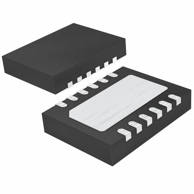
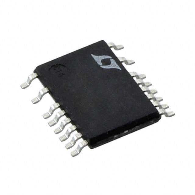
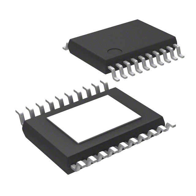
The LT8415EDDB is an ultralow power boost converter with two integrated complementary MOSFET half-bridges (N- and P-channel), integrated power switch, Schottky diode and output disconnect circuitry. The N-channel and P-channel MOSFETs in each half-bridge are synchronously controlled by a single input pin, and never turn on at the same time in typical applications.
The boost regulator controls power delivery by varying both the peak inductor current and switch off-time. This control scheme results in low output voltage ripple as well as high efficiency over a wide load range. The quiescent current is a low 10.5μA, which is further reduced to 0μA in shutdown. The internal disconnect circuitry allows the output voltage to be blocked from the input during shutdown. High value (12.4M/0.4M) resistors are integrated on chip for output voltage detection, significantly reducing input referred quiescent current. The LT8415EDDB also features a comparator built into the SHDN pin, overvoltage protection for the CAP, VOUT, OUT1 and OUT2 pins, built in soft start and comes in a tiny 12-pin 3mm × 2mm DFN package.
Feature
- High Voltage Switches Built in (Dual half-bridge)
- Ultralow Quiescent Current
- 10.5μA in Active Mode
- 0μA in Shutdown Mode
- Comparator Built into SHDN pin
- Low Noise Control Scheme
- Adjustable FB reference voltage
- Wide Input Range: 2.5V to 16V
- Wide Output Range: Up to 40V
- Integrated Power NPN Switch (25mA Current Limit)
- Integrated Schottky Diode
- Integrated Output Disconnect
- High Value (12.4M/0.4M) Feedback Resistor Integrated
- Built in Soft Start (Optional Capacitor from VREF to GND)
- Over Voltage Protection for CAP, VOUT, OUT1 and OUT2 Pins
- 12-Pin 3mm × 2mm DFN package
Applications
- Sensor Power
- RF Mems Relay Power
- Low Power Actuator Bias/Control
- Liquid Lens Driver
(Picture: Pinout)

