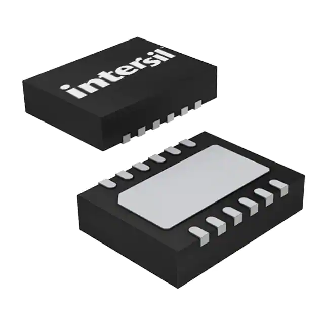
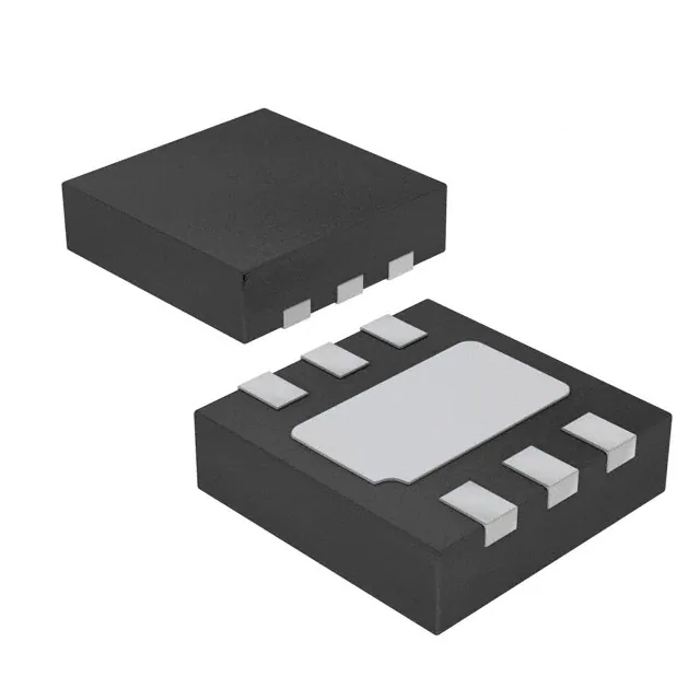
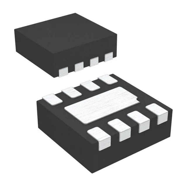
The a 800mA Synchronous buck regulator with an input range 36V. It provides an easy to use, high efficiency low BOM count solution for a variety of applications. The ISL85418FRZ integrates both high-side and low-side NMOS FET's and features a PFM mode for improved efficiency at light loads. This feature can be disabled if forced PWM mode is desired. The part switches at a default frequency of 500kHz but may also be programmed using an external resistor from to 2MHz. The ISL85418FRZ has the ability to utilize internal or external compensation. By integrating both NMOS devices and providing internal configuration options, minimal external components are required, reducing BOM count and complexity of design. With the wide VIN range and reduced, BOM the part provides an easy to implement design solution for a variety of applications while giving superior performance. It will provide a very robust design for high voltage Industrial applications as well as an efficient solution for battery powered applications. The part is available in a small Pb free 4mmx3mm DFN plastic package with an operation temperature range to +125�C.
FeaturesWide input voltage range to 36V Synchronous Operation for high efficiency No compensation required Integrated High-side and Low-side NMOS devices Selectable PFM or forced PWM mode at light loads Internal fixed (500kHz) or adjustable Switching frequency to 2MHz Continuous output current to 800mA Internal or external Soft-start Minimal external components required Power-good and enable functions available.
ApplicationsIndustrial control Medical devices Portable instrumentation Distributed Power supplies Cloud Infrastructure
See "ISL85410EVAL1Z, ISL85418EVAL1Z Wide VIN 1A, 800mA Synchronous Buck Regulator" See "ISL85410DEMO1Z, ISL85418DEMO1Z Wide VIN 1A, 800mA Synchronous Buck Regulator"
CAUTION: These devices are sensitive to electrostatic discharge; follow proper IC Handling Procedures. 1-888-468-3774 | Copyright Intersil Americas LLC 2013, 2014. All Rights Reserved Intersil (and design) is a trademark owned by Intersil Corporation or one of its subsidiaries. All other trademarks mentioned are the property of their respective owners.
Typical Application Schematics. 4 Absolute Maximum Ratings. 6 Thermal Information. 6 Recommended Operating Conditions. 6 Electrical Specifications. 6 Efficiency Curves. 8 Measurements. 10 Detailed Description. Power-On Reset. Soft Start. Power-Good. PWM Control Scheme. Light Load Operation. Output Voltage Selection. Protection Features. Overcurrent Protection. Negative Current Limit. Over-Temperature Protection. Boot Undervoltage Protection. Application Guidelines. Simplifying the Design. Operating Frequency. Synchronization Control. Output Inductor Selection. Buck Regulator Output Capacitor Selection. Loop Compensation Design. Layout Considerations.
Revision History. 20 About Intersil. 20 Package Outline Drawing. 21PIN NUMBER 1 SYMBOL SS PIN DESCRIPTION The SS pin controls the soft-start ramp time of the output. A single capacitor from the SS pin to ground determines the output ramp rate. See "Soft-Start" on page 14 for soft-start details. If the SS pin is tied to VCC, an internal soft-start of 2ms will be used. Synchronization and light load operational mode selection input. Connect to logic high or VCC for PWM mode. Connect to logic low or ground for PFM mode. Logic ground enables the IC to automatically choose PFM or PWM operation. Connect to an external clock source for synchronization with positive edge trigger. Sync source must be higher than the programmed IC frequency. There is an internal 5M pull-down resistor to prevent an undefined logic state if SYNC is left floating. Floating bootstrap supply pin for the power MOSFET gate driver. The bootstrap capacitor provides the necessary charge to turn on the internal N-Channel MOSFET. Connect an external 100nF capacitor from this pin to PHASE. The input supply for the power stage of the regulator and the source for the internal linear bias regulator. Place a minimum of 4.7�F ceramic capacitance from VIN to GND and close to the IC for decoupling. Switch node output. It connects the switching FET's with the external output inductor. Power ground connection. Connect directly to the system GND plane. Regulator enable input. The regulator and bias LDO are held off when the pin is pulled to ground. When the voltage on this pin rises above 1V, the chip is enabled. Connect this pin to VIN for automatic start-up. Do not connect EN pin to VCC since the LDO is controlled by EN voltage. Open drain power-good output that is pulled to ground when the output voltage is below regulation limits or during the soft-start interval. There is an internal 5M internal pull-up resistor. Output of the internal 5V linear bias regulator. Decouple to PGND with a 1�F ceramic capacitor at the pin. Feedback pin for the regulator. FB is the inverting input to the voltage loop error amplifier. COMP is the output of the error amplifier. The output voltage is set by an external resistor divider connected to FB. In addition, the PWM regulator's power-good and UVLO circuits use FB to monitor the regulator output voltage. COMP is the output of the error amplifier. When it is tied to VCC, internal compensation is used. When only an RC network is connected from COMP to GND, external compensation is used. See "Loop Compensation Design" on page 17 for more details. Frequency selection pin. Tie to VCC for 500kHz switching frequency. Connect a resistor to GND for adjustable frequency from to 2MHz. Signal ground connections. Connect to application board GND plane with at least 5 vias. All voltage levels are measured with respect to this pin. The EPAD MUST not float.
Feature
- Wide input voltage range: 3V to 40V
- Synchronous operation for high efficiency
- No compensation required
- Integrated high-side and low-side NMOS devices
- Selectable PFM or forced PWM mode at light loads
- Internal fixed frequency (500kHz) or adjustable switching frequency (300kHz to 2MHz)
- Continuous output current up to 800mA
- Internal or external soft-start
- Minimal external components required
- Power-good and enable functions available

