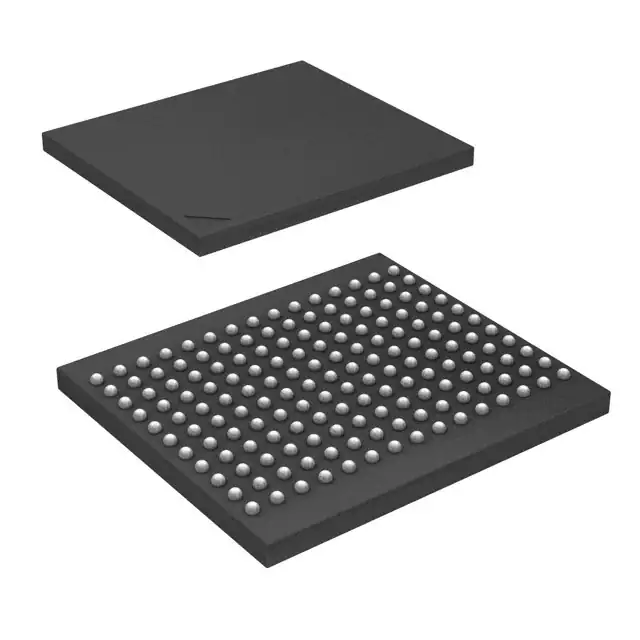
The 71V67603S133BQG 3.3V CMOS SRAM is organized as 256K x 36. The 71V67603S133BQG SRAM contains write, data, address and control registers. The burst mode feature offers the highest level of performance to the system designer, as it can provide four cycles of data for a single address presented to the SRAM.The order of these three addresses are defined by the internal burst counter and the LBO input pin.
Feature
- High system speed 166MHz (3.5ns clock access time)
- LBO input selects interleaved or linear burst mode
- Self-timed write cycle with global write control (GW), byte
- write enable (BWE), and byte writes (BWx)
- 3.3V core power supply
- Power down controlled by ZZ input
- 3.3V I/O supply (VDDQ)
- Available in 100-pin TQFP, 119-pin BGA and 165 fpBGA packages


