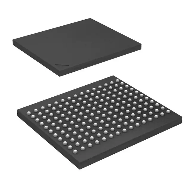
The 71V67903S75BQ 3.3V CMOS SRAM is organized as 512K x 18. The 71V67903S75BQ SRAM contains write, data, address and control registers. There are no registers in the data output path (flow-through architecture). The burst mode feature offers the highest level of performance to the system designer, as it can provide four cycles of data for a single address presented to the SRAM.
Feature
- Fast access times 7.5ns up to 117MHz clock frequency
- LBO input selects interleaved or linear burst mode
- Self-timed write cycle with global write control (GW), byte write enable (BWE), and byte writes (BWx)
- 3.3V core power supply
- Power down controlled by ZZ input
- 3.3V I/O supply (VDDQ)
- Available in 100-pin TQFP, 119-pin BGA and 165 fpBGA packages


