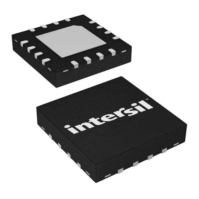
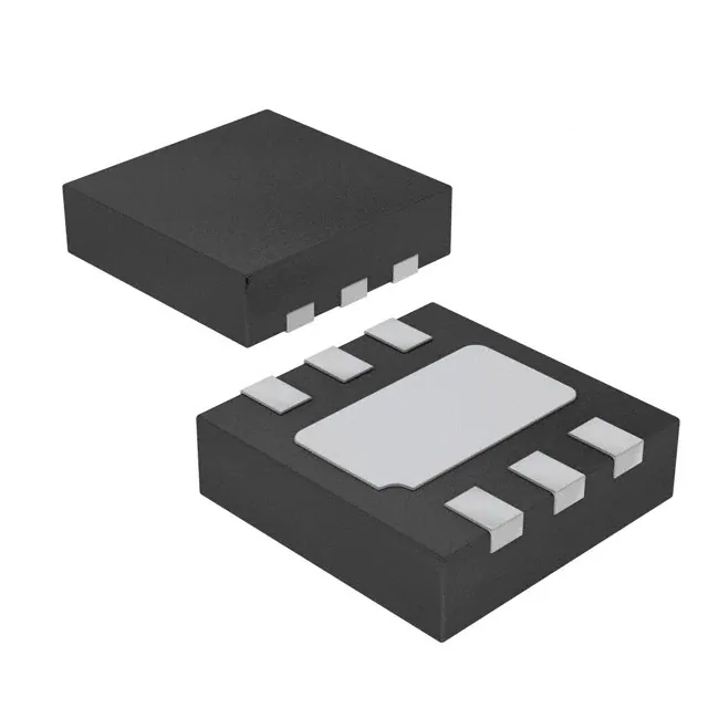
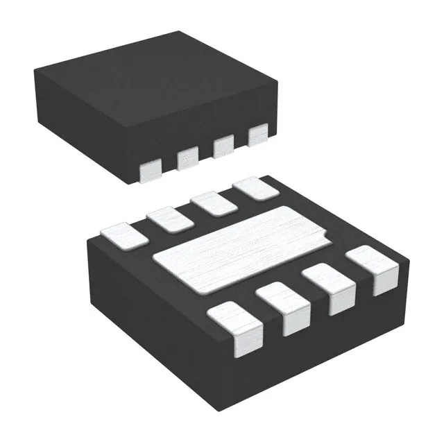
The ISL8025, ISL8025A are highly efficient, monolithic, synchronous step-down DC/DC converters that can deliver 5A of continuous output current from to 5.5V input supply. The devices use current mode control architecture to deliver a very low duty cycle operation at high frequency with fast transient response and excellent loop stability. The ISL8025, ISL8025A integrates a very low ON-resistance P-Channel (45m) high-side FET and N-Channel (19m) low-side FET to maximize efficiency and minimize external component count. The 100% duty-cycle operation allows less than 225mV dropout voltage at 5A output current. The operation frequency of the pulse-width modulator (PWM) is adjustable from to 4MHz. The default switching frequency, which is set by connecting the FS pin high, is 1MHz for the ISL8025IRTAJZ-T7A and 2MHz for the ISL8025A. The ISL8025, ISL8025A can be configured for discontinuous or forced continuous operation at light load. Forced continuous operation reduces noise and RF interference, while discontinuous mode provides higher efficiency by reducing switching losses at light loads. Fault protection is provided by internal hiccup mode current limiting during short circuit and overcurrent conditions. Other protection, such as overvoltage and over-temperature, are also integrated into the device. A power-good output voltage monitor indicates when the output is in regulation. The ISL8025, ISL8025A offers a 1ms Power-good (PG) timer at power-up. When in shutdown, the ISL8025, ISL8025A discharges the output capacitor through an internal soft-stop switch. Other features include internal fixed or adjustable soft-start and internal/external compensation. The ISL8025, ISL8025A are offered in a space saving Ld 3x3 Pb-free QFN package with an exposed pad for improved thermal performance and 1mm maximum height. The complete converter occupies less than 0.22 in2 area.
Featuresto 5.5V input voltage range Very low ON-resistance FET's - P-channel 45m and N-channel 19m typical values High efficiency synchronous buck regulator with to 95% efficiency Pin-to-pin compatible with ISL8023 and ISL8024 0.8% reference accuracy over-temperature/load/line Complete BOM with as few as 3 external parts Internal soft-start: 1ms or adjustable Soft-stop output discharge during disable Adjustable frequency from 4MHz - default 2MHz (ISL8025A) External synchronization to 4MHz Over-temperature, overcurrent, overvoltage and negative overcurrent protection
ApplicationsDC/DC POL modules C/�P, FPGA and DSP power Plug-in DC/DC modules for routers and switchers Portable instruments Test and measurement systems Li-ion battery powered devices
See AN1806, "5A Low Quiescent Current High Efficiency Synchronous Buck Regulator"L1 VIN 16 PHASE 15 PHASE 14 PHASE x 22�F PGND 12 PGND 11 SGND 9 8 COMP PAD 100k +0.6V
*C3 IS OPTIONAL. IT IS RECOMMENDED TO PUT A PLACEHOLDER FOR IT AND CHECK LOOP ANALYSIS BEFORE USE.
FIGURE 1. TYPICAL APPLICATION CIRCUIT CONFIGURATION (INTERNAL COMPENSATION OPTION)
CAUTION: These devices are sensitive to electrostatic discharge; follow proper IC Handling Procedures. 1-888-468-3774 | Copyright Intersil Americas LLC 2013. All Rights Reserved Intersil (and design) is a trademark owned by Intersil Corporation or one of its subsidiaries. All other trademarks mentioned are the property of their respective owners.
Pin Configuration. 3 Pin Descriptions. 3 Ordering Information. 4 Absolute Maximum Ratings. 6 Thermal Information. 6 Recommended Operating Conditions. 6 Electrical Specifications. 6 Typical Operating Performance. 8 Typical Operating Performance. 11 Theory of Operation. 16 PWM Control Scheme. SKIP Mode. Frequency Adjust. Overcurrent Protection. Negative Current Protection. PG. UVLO. Soft Start-Up. Enable. Discharge Mode (Soft-Stop). Power MOSFETs. 100% Duty Cycle. Thermal Shut-Down. Output Inductor and Capacitor Selection. Output Voltage Selection. Input Capacitor Selection. Loop Compensation Design.
PCB Layout Recommendation. 20 Revision History. 20 About Intersil. 20 Package Outline Drawing. 21DESCRIPTION Input supply voltage. Place a minimum of two 22�F ceramic capacitors from VIN to PGND as close as possible to the IC for decoupling. Input supply voltage for the logic. Connect VIN pin. Power-good is an open-drain output. Use to 100k pull-up resistor connected between VIN and PG. At power-up or EN HI, PG rising edge is delayed by 1ms upon output reached within regulation. Mode Selection pin. Connect to logic high or input voltage VIN for PWM mode. Connect to logic low or ground for PFM mode. Connect to an external function generator for synchronization with the positive edge trigger. There is an internal 1M pull-down resistor to prevent an undefined logic state in case of SYNC pin float. Regulator enable pin. Enable the output when driven to high. Shutdown the chip and discharge output capacitor when driven to low. This pin sets the oscillator switching frequency, using a resistor, RFS, from the FS pin to GND. The frequency of operation may be programmed between to 4MHz. The default frequency FS is connected to VIN. SS is used to adjust the soft-start time. Set to SGND for internal 1ms rise time. Connect a capacitor from SS to SGND to adjust the soft-start time. Do not use more than 33nF per IC. The feedback network of the regulator, FB, is the negative input to the transconductance error amplifier. COMP is the output of the amplifier if COMP is not tied to VDD. Otherwise, COMP is disconnected thru a MOSFET for internal compensation. Must connect COMP to VDD in internal compensation mode. The output voltage is set by an external resistor divider connected to FB. With a properly selected divider, the output voltage can be set to any voltage between the power rail (reduced by converter losses) and the 0.6V reference. There is an internal compensation to meet a typical application. Additional external networks across COMP and SGND might be required to improve the loop compensation of the amplifier operation. In addition, the regulator power-good and undervoltage protection circuitry use FB to monitor the regulator output voltage. Signal ground. Power ground. Switching node connections. Connect to one terminal of the inductor. This pin is discharged a 100 resistor when the device is disabled. See"FUNCTIONAL BLOCK DIAGRAM" on page 5 for more detail. The exposed pad must be connected to the SGND pin for proper electrical performance. Place as many vias as possible under the pad connecting to SGND plane for optimal thermal performance.
Feature
- 2.7V to 5.5V input voltage range
- Very low ON-resistance FET’s - P-channel 36mΩ and N-channel 13mΩ typical values
- High efficiency synchronous buck regulator with up to 95% efficiency
- Pin-to-pin compatible with ISL8023 and ISL8024
- 0.8% reference accuracy over-temperature/load/line
- Internal soft-start: 1ms or adjustable
- Soft-stop output discharge during disable
- Adjustable frequency from 500kHz to 4MHz - default at 1MHz (ISL8025), 2MHz (ISL8025A)
- External synchronization up to 4MHz
- Over-temperature, overcurrent, overvoltage and negative overcurrent protection

