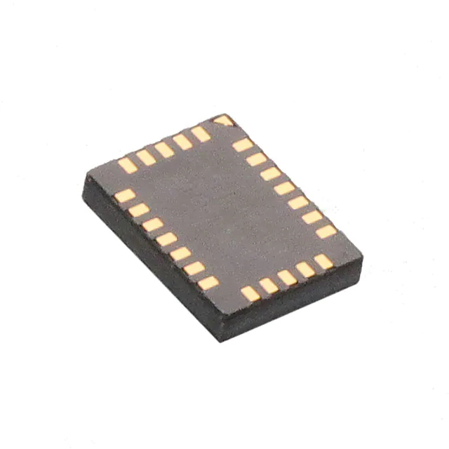
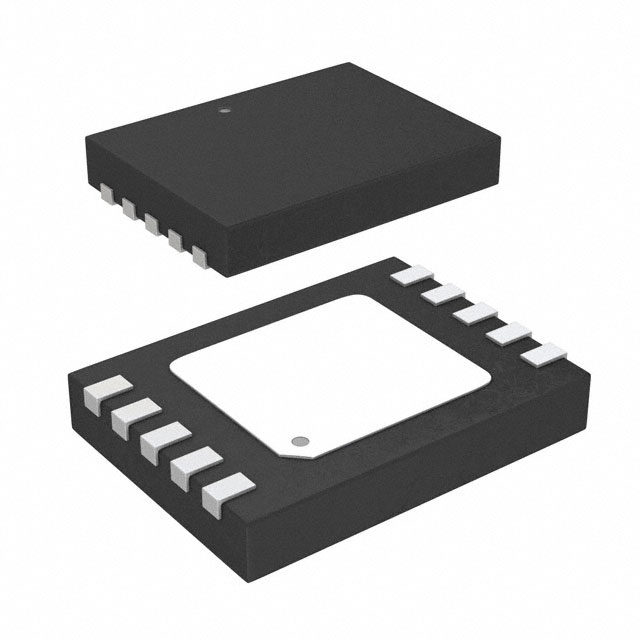
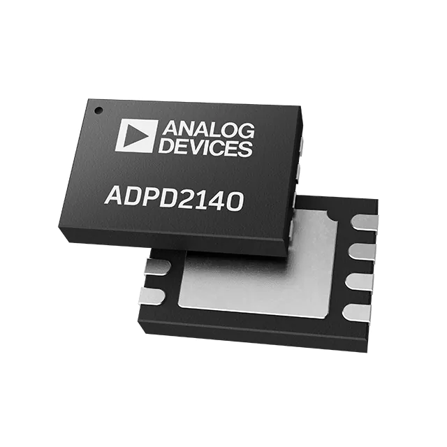
The ADP2140ACPZ1218R7 includes a high efficiency, low quiescent 600 mAstepdown dc-to-dc converter and a 300 mA LDO packaged in asmall 10-lead 3 mm × 3 mm LFCSP. The total solution requiresonly four tiny external components.
The buck regulator uses a proprietary high speed current-mode,constant frequency, pulse-width modulation (PWM) controlscheme for excellent stability and transient response. To ensurethe longest battery life in portable applications, the ADP2140ACPZ1218R7 hasa power saving variable frequency mode to reduce switching frequencyunder light loads.
The LDO is a low quiescent current, low dropout linear regulatordesigned to operate in a split supply mode with VIN2 as low as1.65 V. The low input voltage minimum allows the LDO to bepowered from the output of the buck regulator increasing efficiencyand reducing power dissipation. The ADP2140ACPZ1218R7 runs frominput voltages of 2.3 V to 5.5 V allowing single Li+/Li− polymer cell, multiple alkaline/NiMH cell, PCMCIA, and other standardpower sources.
ADP2140ACPZ1218R7 includes a power-good pin, soft start, and internal compensation. Numerous power sequencing options are user-selectable through two enable inputs. In autosequencing mode, the highest voltage output enables on the rising edge of EN1. During logic controlled shutdown, the input disconnects from the output and draws less than 300 nA from the input source. Other key features include: undervoltage lockout to prevent deep battery discharge, soft start to prevent input current overshoot at startup, and both short-circuit protection and thermal overload protection circuits to prevent damage in adverse conditions.
When the ADP2140ACPZ1218R7 is used with two 0603 capacitors, one 0402capacitor, one 0402 resistor, and one 0805 chip inductor, the totalsolution size is approximately 90 mm2 resulting in the smallest footprintsolution to meet a variety of portable applications.
Applications- Mobile phones
- Personal media players
- Digital camera and audio devices
- Portable and battery-powered equipment
Feature
- Input voltage range: 2.3 V to 5.5 V
- LDO input (VIN2) 1.65 V to 5.5 V
- Buck output voltage range: 1.0 V to 3.3 V
- LDO output voltage range: 0.8 V to 3.3 V
- Buck output current: 600 mA
- LDO output current: 300 mA
- LDO quiescent current: 22 μA with zero load
- Buck quiescent current: 20 μA in PSM mode
- Low shutdown current: <0.3 μA
- Low LDO dropout 110 mV @ 300 mA load
- High LDO PSRR
- 65 dB @ 10 kHz at VOUT2 = 1.2 V
- 55 dB @ 100 kHz at VOUT2 = 1.2 V
- Low noise LDO: 40 μV rms at VOUT2 = 1.2 V
- Initial accuracy: ±1%
- Current-limit and thermal overload protection
- Power-good indicator
- Optional enable sequencing
- 10-lead 0.75 mm × 3 mm × 3 mm LFCSP package
Applications
- Mobile phones
- Personal media players
- Digital camera and audio devices
- Portable and battery-powered equipment
(Picture: Pinout)


