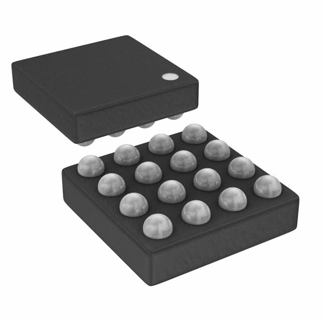
The ADP5033ACBZ-2-R7 combines two high performance buck regulators and two low dropout regulators (LDO) in a tiny, 16-ball, 2 mm × 2 mm WLCSP to meet demanding performance and board space requirements.
The high switching frequency of the buck regulators enables tiny multilayer external components and minimizes the board space. When the MODE pin is set high, the buck regulators operate in forced PWM mode.When the MODE pin is set low, the buck regulators operate in forced power save mode (PSM). When the load is around the nominal value and the load current falls below a predefined threshold, the regulator operates in PSM, improving the light load efficiency.
The two bucks operate out of phase to reduce the input capacitor requirement and noise.
The low quiescent current, low dropout voltage, and wide input voltage range of the ADP5033ACBZ-2-R7 LDO extend the battery life of portable devices. The ADP5033ACBZ-2-R7 LDOs maintain power supply rejection greater than 60 dB for frequencies as high as 10 kHz while operating with a low headroom voltage.
The regulators in the ADP5033ACBZ-2-R7 are activated by the ENA and ENB pins. The specific channels controlled by ENA and ENB are set by factory programming. A high voltage level applied to the enable pins activates the regulators. The default output voltages are factory programmable and can be set to a wide range of options.
Feature
- Input voltage range: 2.3 V to 5.5 V
- Two 800 mA buck regulators and two 300 mA LDOs
- Tiny, 16-ball, 2 mm × 2 mm WLCSP package
- Regulator accuracy: ±1.8%
- Factory programmable VOUTx
- 3 MHz buck operation with forced PWM and auto PWM/PSM modes
- BUCK1/BUCK2: output voltage range from 0.8 V to 3.3 V
- LDO1/LDO2: output voltage range from 0.8 V to 3.3V
- LDO1/LDO2: low input supply voltage from 1.7 V to 5.5 V
- LDO1/LDO2: high PSRR and low output noise
Applications
- Power for processors, ASICS, FPGAs, and RF chipsets
- Portable instrumentation and medical devices
- Space constrained devices
(Picture: Pinout)

