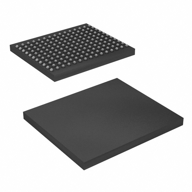
The CY7C13101KV18, CY7C13251KV18, CY7C13121KV18, and CY7C13141KV18 are 1.8 V Synchronous Pipelined SRAMs, equipped with QDR II architecture. QDR II architecture consists of two separate ports: the read port and the write port to access the memory array. The read port has dedicated data outputs to support read operations and the write port has dedicated data inputs to support write operations. QDR II architecture has separate data inputs and data outputs to completely eliminate the need to “turnaround” the data bus that exists with common I/O devices. Access to each port is through a common address bus. Addresses for read and write addresses are latched on alternate rising edges of the input (K) clock. Accesses to the QDR II read and write ports are completely independent of one another. To maximize data throughput, both read and write ports are equipped with DDR interfaces. Each address location is associated with two 8-bit words (CY7C13101KV18), 9-bit words (CY7C13251KV18), 18-bit words (CY7C13121KV18), or 36-bit words (CY7C13141KV18) that burst sequentially into or out of the device. Because data can be transferred into and out of the device on every rising edge of both input clocks (K and K and C and C), memory bandwidth is maximized while simplifying system design by eliminating bus turnarounds. Depth expansion is accomplished with port selects, which enables each port to operate independently. All synchronous inputs pass through input registers controlled by the K or K input clocks. All data outputs pass through output registers controlled by the C or C (or K or K in a single clock domain) input clocks. Writes are conducted with on-chip synchronous self-timed write circuitry. These devices are down bonded from the 65 nm 72M QDRII+/DDRII+ devices and hence have the same IDD/ISB1 values and the same JTAG ID code as the equivalent 72M device options. For details refer to the application note AN53189, 65 nm Technology Interim QDRII+/DDRII+ SRAM device family description.
Features
■ Separate independent read and write data ports ❐ Supports concurrent transactions
■ 333 MHz clock for high bandwidth
■ 2-word burst on all accesses
■ Double data rate (DDR) interfaces on both read and write ports(data transferred at 666 MHz) at 333 MHz
■ Two input clocks (K and K) for precise DDR timing ❐ SRAM uses rising edges only
■ Two input clocks for output data (C and C) to minimize clock skew and flight time mismatches
■ Echo Clocks (CQ and CQ) simplify data capture in high speed systems
■ Single multiplexed address input bus latches address inputs for both read and write ports
■ Separate port selects for depth expansion
■ Synchronous internally self-timed writes
■ QDR® II operates with 1.5 cycle read latency when DOFF is asserted HIGH
■ Operates similar to QDR I device with one cycle read latency when DOFF is asserted LOW
■ Available in ×8, ×9, ×18, and ×36 configurations
■ Full data coherency, providing most current data
■ Core VDD = 1.8 V (±0.1 V); I/O VDDQ = 1.4 V to VDD ❐ Supports both 1.5 V and 1.8 V I/O supply
■ Available in 165-ball fine pitch ball grid array (FBGA) package (13 × 15 × 1.4 mm)
■ Offered in both Pb-free and non Pb-free packages
■ Variable drive HSTL output buffers
■ JTAG 1149.1 compatible test access port
■ Phase locked loop (PLL) for accurate data placement
Feature
• True Dual-Ported memory cells which allow simultaneous reads of the same memory location
• 1K x 8 organization
• 0.65-micron CMOS for optimum speed/power
• High-speed access: 15 ns
• Low operating power: ICC = 110 mA (max.)
• Fully asynchronous operation
• Automatic power-down
• Master CY7C130/CY7C131 easily expands data bus width to 16 or more bits using slave CY7C140/CY7C141
• BUSY output flag on CY7C130/CY7C131; BUSY input on CY7C140/CY7C141
• INT flag for port-to-port communication
• Available in 48-pin DIP (CY7C130/140), 52-pin PLCC, 52-Pin TQFP.
• Pb-Free packages available
(Picture:Pinout / Diagram)