Functional Description
The CY7C1049CV33 is a high performance CMOS Static RAM organized as 524,288 words by eight bits. Easy memory expansion is provided by an active LOW Chip Enable (CE), an active LOW Output Enable (OE), and three-state drivers. Writing to the device is accomplished by taking Chip Enable (CE) and Write Enable (WE) inputs LOW. Data on the eight I/O pins (I/O0 through I/O7) is then written into the location specified on the address pins (A0 through A18).
Reading from the device is accomplished by taking Chip Enable (CE) and Output Enable (OE) LOW while forcing Write Enable (WE) HIGH. Under these conditions, the contents of the memory location specified by the address pins appear on the I/O pins.
The eight input and output pins (I/O0 through I/O7) are placed in a high impedance state when the device is deselected (CE HIGH), the outputs are disabled (OE HIGH), or during a write operation (CE LOW, and WE LOW).
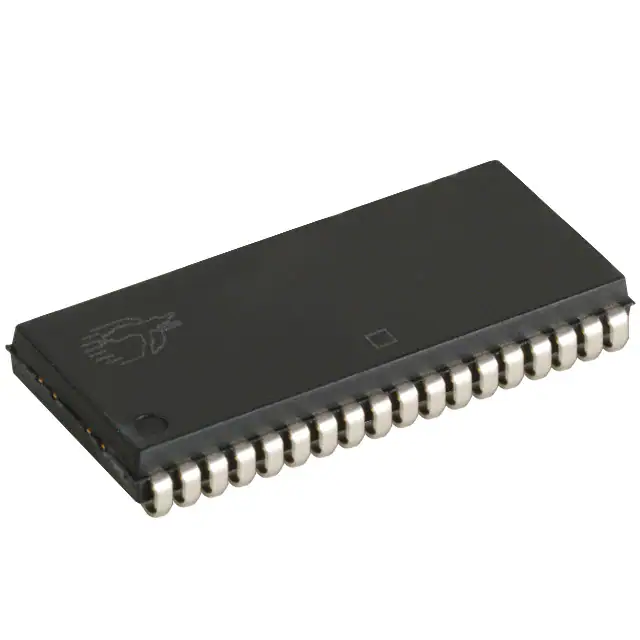
The CY7C1049CV33 is available in standard 400-mil-wide 36-pin SOJ package and 44-pin TSOP II package with center power and ground (revolutionary) pinout.
For best practice recommendations, refer to the Cypress application note AN1064, SRAM System Guidelines.
Features
■ Temperature ranges
❐ Commercial: 0°C to 70°C
❐ Industrial/Automotive -A: –40°C to 85°C
❐ Automotive-E: –40°C to 125°C
■ High Speed
❐ tAA = 10 ns
■ Low Active Power
❐ 324 mW (max)
■ 2.0V Data Retention
■ Automatic Power Down when Deselected
■ TTL-compatible Inputs and Outputs
■ Easy Memory Expansion with CE and OE features
(Picture: Pinout)