The ADP7142AUJZ-R7 is a CMOS, low dropout (LDO) linear regulatorthat operates from 2.7 V to 40 V and provides up to 200 mA ofoutput current. This high input voltage LDO is ideal for theregulation of high performance analog and mixed signal circuitsoperating from 40 V down to 1.2 V rails. Using an advancedproprietary architecture, the device provides high power supplyrejection, low noise, and achieves excellent line and load transientresponse with a small 2.2 μF ceramic output capacitor. TheADP7142AUJZ-R7 regulator output noise is 11 μV rms independent ofthe output voltage for the fixed options of 5 V or less.
The ADP7142AUJZ-R7 is available in 15 fixed output voltage options.The following voltages are available from stock: 1.2 V (adjustable),1.8 V, 2.5 V, 3.3 V, 3.8 V, and 5.0 V. Additional voltages available by special order are 1.5 V, 1.85 V, 2.0 V, 2.2 V, 2.75 V, 2.8 V, 2.85 V,4.2 V, and 4.6 V.
Each fixed output voltage can be adjusted above the initial setpoint with an external feedback divider. This allows the ADP7142to provide an output voltage from 1.2 V to VIN − VDO with highPSRR and low noise.
User programmable soft start with an external capacitor isavailable in the LFCSP and SOIC packages.
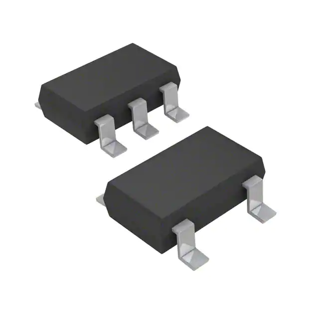
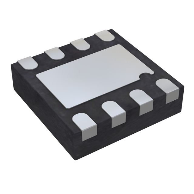
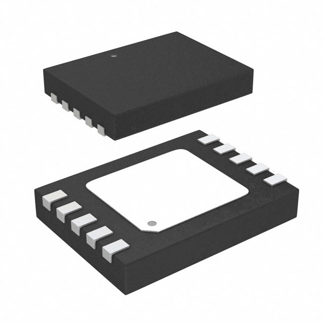
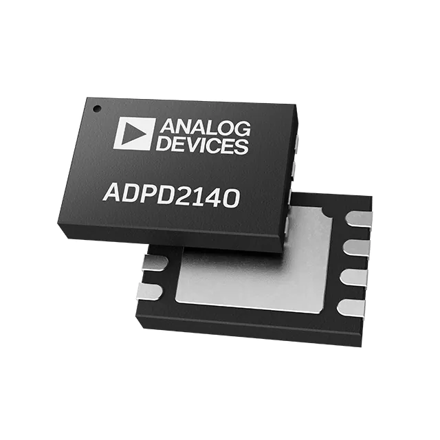
The ADP7142AUJZ-R7 is available in a 6-lead, 2 mm × 2 mm LFCSPmaking it not only a very compact solution, but it also providesexcellent thermal performance for applications requiring up to200 mA of output current in a small, low profile footprint. TheADP7142AUJZ-R7 is also available in a 5-lead TSOT and an 8-lead SOIC.
Feature
- Low noise: 11 μV rms independent of fixed output voltage
- PSRR of 88 dB at 10 kHz, 68 dB at 100 kHz, 50 dB at 1 MHz, VOUT ≤ 5 V, VIN = 7 V
- Input voltage range: 2.7 V to 40 V
- Maximum output current: 200 mA
- Initial accuracy: ±0.8%
- Accuracy over line, load, and temperature
- −1.2% to +1.5%, TJ = −40°C to +85°C
- ±1.8%, TJ = −40°C to +125°C
- Low dropout voltage: 200 mV (typical) at a 200 mA load, VOUT = 5 V
- User programmable soft start (LFCSP and SOIC only)
- Low quiescent current, IGND = 50 μA (typical) with no load
- Low shutdown current: 1.8 μA at VIN = 5 V, 3.0 μA at VIN = 40 V
- Stable with a small 2.2 μF ceramic output capacitor
- Fixed output voltage options: 1.8 V, 2.5 V, 3.3 V, 3.8 V, and 5.0 V
- 15 standard voltages between 1.2 V and 5.0 V are available
- Adjustable output from 1.2 V to VIN – VDO, output can be adjusted above initial set point
- Precision enable
- 2 mm × 2 mm, 6-lead LFCSP, 8-Lead SOIC, 5-Lead TSOT
- Supported bytool
Applications
- Regulation to noise sensitive applications
- ADC, DAC circuits, precision amplifiers, power for VCO VTUNE control
- Communications and infrastructure
- Medical and healthcare
- Industrial and instrumentation
(Picture: Pinout)

