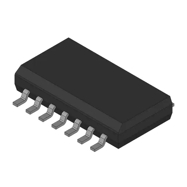
The TL497ACNS incorporates all the active functions required in the construction of switching voltage regulators. It also can be used as the control element to drive external components for high-power-output applications. The TL497ACNS was designed for ease of use in step-up, step-down, or voltage-inversion applications requiring high efficiency.
The TL497ACNS is a fixed-on-time variable-frequency switching-voltage-regulator control circuit. The switch-on time is programmed by a single external capacitor connected between FREQ CONTROL and GND. This capacitor, CT, is charged by an internal constant-current generator to a predetermined threshold. The charging current and the threshold vary proportionally with VCC. Thus, the switch-on time remains constant over the specified range of input voltage (4.5 V to 12 V). Typical on times for various values of CT are as follows:
TIMING CAPACITOR, CT (pF)200250350400500750100015002000ON TIME (μs)19222632445680120180The output voltage is controlled by an external resistor ladder network (R1 and R2 in Figures 1, 2, and 3) that provides a feedback voltage to the comparator input. This feedback voltage is compared to the reference voltage of 1.2 V (relative to SUBSTRATE) by the high-gain comparator. When the output voltage decays below the value required to maintain 1.2 V at the comparator input, the comparator enables the oscillator circuit, which charges and discharges CT as described above. The internal pass transistor is driven on during the charging of CT. The internal transistor can be used directly for switching currents up to 500 mA. Its collector and emitter are uncommitted, and it is current driven to allow operation from the positive supply voltage or ground. An internal Schottky diode matched to the current characteristics of the internal transistor also is available for blocking or commutating purposes. The TL497ACNS also has on-chip current-limit circuitry that senses the peak currents in the switching regulator and protects the inductor against saturation and the pass transistor against overstress. The current limit is adjustable and is programmed by a single sense resistor, RCL, connected between VCC and CUR LIM SENS. The current-limit circuitry is activated when 0.7 V is developed across RCL. External gating is provided by the INHIBIT input. When the INHIBIT input is high, the output is turned off.
Simplicity of design is a primary feature of the TL497A. With only six external components (three resistors, two capacitors, and one inductor), the TL497ACNS operates in numerous voltage-conversion applications (step-up, step-down, invert) with as much as 85% of the source power delivered to the load. The TL497ACNS replaces the TL497 in all applications.
The TL497AC is characterized for operation from 0°C to 70°C. The TL497AI is characterized for operation from -40°C to 85°C.
Feature
- High Efficiency . . . 60% or Greater
- Peak Switch Current . . . 500 mA
- Input Current Limit Protection
- TTL-Compatible Inhibit
- Adjustable Output Voltage
- Input Regulation . . . 0.2% Typ
- Output Regulation . . . 0.4% Typ
- Soft Start-Up Capability
- Can be Used in Buck, Boost, and Inverting Configurations


