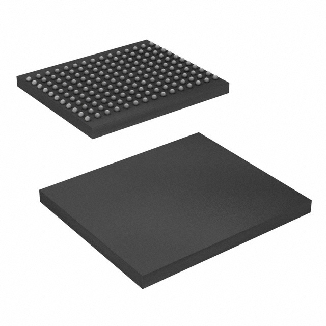
The CY7C1371D/CY7C1373D is a 3.3V, 512K x 36/1 Mbit x 18 Synchronous Flow-through Burst SRAM designed specifically to support unlimited true back-to-back Read/Write operations without the insertion of wait states. The CY7C1371D/ CY7C1373D is equipped with the advanced No Bus Latency (NoBL) logic required to enable consecutive Read/Write operations with data being transferred on every clock cycle. This feature dramatically improves the throughput of data through the SRAM, especially in systems that require frequent Write-Read transitions.
Feature
• No Bus Latency™ (NoBL™) architecture eliminates dead cycles between write and read cycles
• Can support up to 133-MHz bus operations with zero wait states
— Data is transferred on every clock
• Pin-compatible and functionally equivalent to ZBT™ devices
• Internally self-timed output buffer control to eliminate the need to use OE
• Registered inputs for flow-through operation
• Byte Write capability
• 3.3V/2.5V I/O power supply
• Fast clock-to-output times
— 6.5 ns (for 133-MHz device)
— 8.5 ns (for 100-MHz device)
• Clock Enable (CEN) pin to enable clock and suspend operation
• Synchronous self-timed writes
• Asynchronous Output Enable
• Offered in JEDEC-standard lead-free 100 TQFP, 119-ball BGA and 165-ball fBGA packages
• Three chip enables for simple depth expansion
• Automatic Power-down feature available using ZZ mode or CE deselect
• JTAG boundary scan for BGA and fBGA packages
• Burst Capability—linear or interleaved burst order
• Low standby power