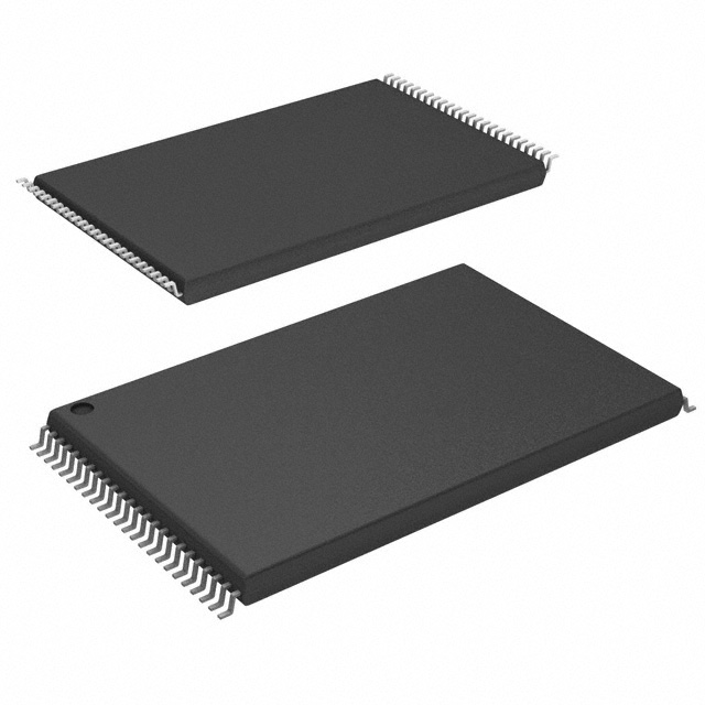
The S29PL064J70BFI120 is a 64MB CMOS simultaneous Read/Write Flash Memory with Enhanced VersatileIO™ Control. This device is organized as 8M words. The word-wide data (x16) appears on DQ15-DQ0. This device can be programmed in-system or in standard EPROM programmers. A 12V VPP is not required for write or erase operations. The device offers fast page access times of 20 to 30ns, with corresponding random access time of 70ns respectively, allowing high speed microprocessors to operate without wait states. To eliminate bus contention the device has separate chip enable (CE#), write enable (WE#) and output enable (OE#) controls.
Feature
- Single power supply operation
- Dual chip enable inputs - Two CE# inputs control selection of each half of the memory space
- Data can be continuously read from one bank while executing erase/program functions in another bank
- Simultaneous read/write operation - Zero latency switching from write to read operations
- Secured silicon sector region
- Both top and bottom boot blocks in one device
- Manufactured on 110nm process technology
- Data retention - 20 years typical
- Cycling endurance - 1million cycles per sector typical
- High performance
- Power consumption
- Software command-set compatible with JEDEC 42.4 standard
- Erase suspend/erase resume
- Program suspend/program resume
- Unlock bypass program command
- Reduces overall programming time when issuing multiple program command sequences
- Ready/busy# pin - Provides a hardware method of detecting program or erase cycle completion
- Hardware reset pin - Hardware method to reset the device to reading array data
- WP#/ ACC input
- Persistent sector protection - Sectors can be locked and unlocked in-system at VCC level