1. GENERAL DESCRIPTION
The W29N01HVXINF (1G-bit) NAND Flash memory provides a storage solution for embedded systems with limited space, pins and power. It is ideal for code shadowing to RAM, solid state applications and storing media data such as, voice, video, text and photos. The device operates on a single 2.7V to 3.6V power supply with active current consumption as low as 25mA 10uA for CMOS standby current.
The memory array totals 138,412,032 bytes, and organized into 1,024 erasable blocks of 135,168 bytes. Each block consists of 64 programmable pages of 2,112-bytes each. Each page consists of 2,048-bytes for the main data storage area and 64-bytes for the spare data area (The spare area is typically used for error management functions).
The W29N01HVXINF supports the standard NAND flash memory interface using the multiplexed 8-bit bus to transfer data, addresses, and command instructions. The five control signals, CLE, ALE, #CE, #RE and #WE handle the bus interface protocol. Also, the device has two other signal pins, the #WP (Write Protect) and the RY/#BY (Ready/Busy) for monitoring the device status.
2. FEATURES
· Basic Features
- Density:1Gbit(Single chip solution)
- Vcc:2.7V to 3.6V
- Bus width:×8
- Operating temperature
· Industrial:-40°℃ to 85℃
· Single-Level Cell(SLC) technology.
· Organization
- Density:1G-bit/128M-byte
- Page size
· 2,112 bytes(2048+64 bytes)
- Block size
· 64pages(128K+4K bytes)
· Highest Performance
- Read performance(Max.)
· Random read:25us
· Sequential read cycle:25ns
- Write Erase performance
· Page program time:250us(typ.)
· Block erase time:2ms(typ.)
- Endurance 100,000 Erase/Program Cycles
- 10-years data retention
· Command set
- Standard NAND command set
- Additional command support
· Copy Back
· Lowest power consumption
- Read:25mA(typ.3V),
- Program/Erase:25mA(typ.3V),
- CMOS standby:10uA(typ.)
· Space Efficient Packaging
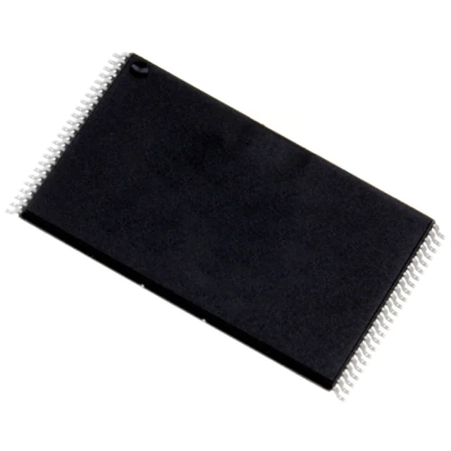
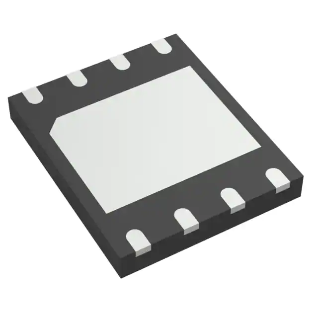
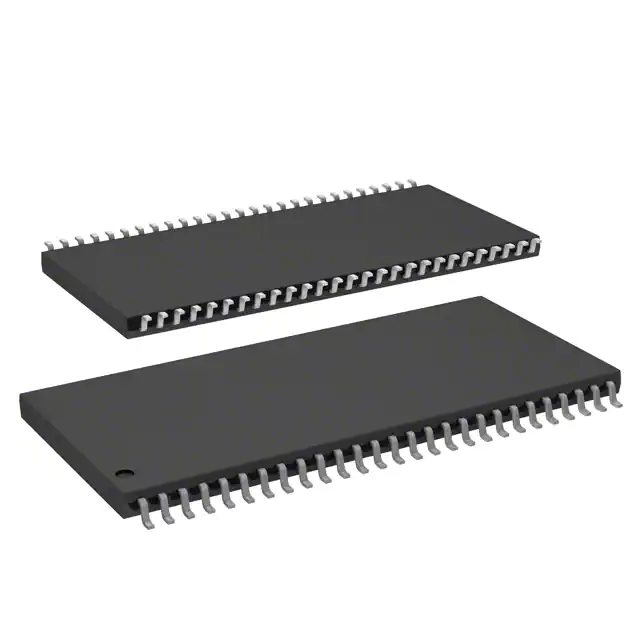
- 48-pin standard TSOP1
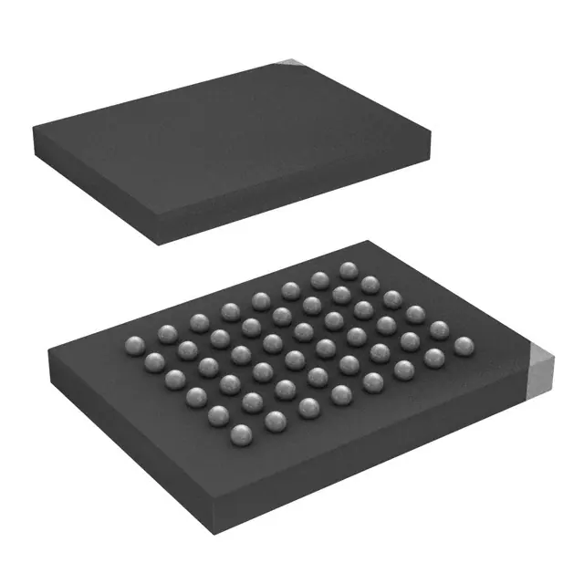
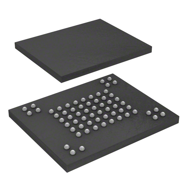
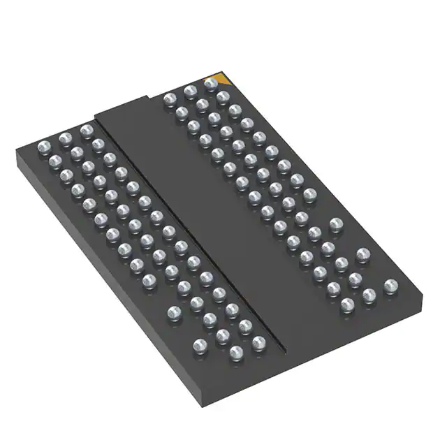
- 48-ball VFBGA-63-ball VFBGA
- Contact Winbond for stacked packages/KGD
(Picture: Pinout)


