• Serial Peripheral Interface (SPI) with Multi-I/O
❐ SPI Clock polarity and phase modes 0 and 3
❐ Command subset and footprint compatible with S25FL-K
Read
❐ Normal Read (Serial):
• 50 MHz clock rate (40 °C to +85 °C/105 °C)
❐ Fast Read (Serial):
• 108 MHz clock rate (40 °C to +85 °C/105 °C)
❐ Dual Read:
• 108 MHz clock rate (40 °C to +85 °C/105 °C)
❐ Quad Read:
• 108 MHz clock rate (40 °C to +85 °C/105 °C)
❐ 54 MB/s maximum continuous data transfer rate 40 °C to +85 °C/105 °C)
❐ Efficient Execute-In-Place (XIP)
❐ Continuous and wrapped read modes
❐ Serial Flash Discoverable Parameters (SFDP)
Program
❐ Serial-input Page Program (up to 256 bytes)
❐ Program Suspend and Resume
Erase
❐ Uniform sector erase (4 kB)
❐ Uniform block erase (64 kB)
❐ Chip erase
❐ Erase Suspend and Resume
Cycling Endurance
❐ 100K Program-Erase cycles, minimum
Data Retention
❐ 20-year data retention, minimum
Security
❐ Three 256-byte Security Registers with OTP protection
❐ Low supply voltage protection of the entire memory
❐ Pointer-based security protection feature (S25FL164K)
❐ Top / Bottom relative Block Protection Range, 4 kB to all of memory
❐ 8-Byte Unique ID for each device
❐ Nonvolatile Status Register bits control protection modes
• Software command protection
• Hardware input signal protection
• Lock-Down until power cycle protection
• OTP protection of security registers
90 nm Floating Gate Technology
Single Supply Voltage
❐ 2.7 V to 3.6 V (Industrial, Industrial Plus, and Extended temperature range)
❐ 2.6 V to 3.6 V (Extended temperature range)
Temperature Ranges
❐ Industrial (40 °C to +85 °C)
❐ Industrial Plus (40 °C to +105 °C)
❐ Automotive, AEC-Q100 Grade 3 (–40°C to +85°C)
❐ Automotive, AEC-Q100 Grade 2 (–40°C to +105°C)
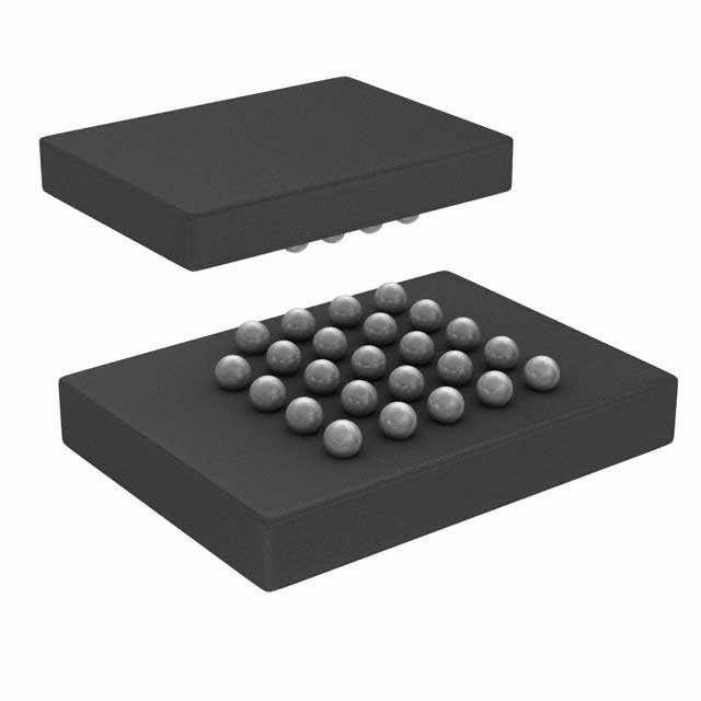
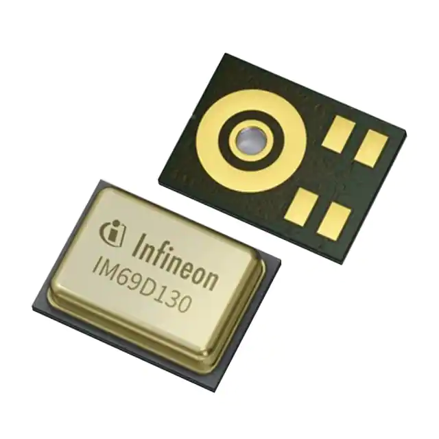
❐ S25FL164K
• 8-lead SOIC (208 mil) – SOC008
• 16-lead SOIC (300 mil) – SO3016
• 8-contact WSON 5 mm 6 mm – WND008
• 24-ball BGA 6 mm 8 mm – FAB024 and FAC024
Description
The S25FL1-K of nonvolatile flash memory devices connect to a host system via a Serial Peripheral Interface (SPI). Traditional SPI single bit serial input and output (Single I/O or SIO) is supported as well as optional two bit (Dual I/O or DIO) and four bit (Quad I/O or QIO) serial protocols. This multiple width interface is called SPI Multi-I/O or MIO.
The SPI-MIO protocols use only 4 to 6 signals:
Chip Select (CS#)
Serial Clock (SCK)
❐ IO0 (SI)
❐ IO1 (SO)
❐ IO2 (WP#)
❐ IO3 (HOLD#)
Serial Data
The SIO protocol uses Serial Input (SI) and Serial Output (SO) for data transfer. The DIO protocols use IO0 and IO1 to input or
output two bits of data in each clock cycle.
The Write Protect (WP#) input signal option allows hardware control over data protection. Software controlled commands can also manage data protection.
The HOLD# input signal option allows commands to be suspended and resumed on any clock cycle.
The QIO protocols use all of the data signals (IO0 to IO3) to transfer 4 bits in each clock cycle. When the QIO protocols are enabled the WP# and HOLD# inputs and features are disabled.
Clock frequency of up to 108 MHz is supported, allowing data transfer rates up to:
Single bit data path = 13.5 Mbytes/s
Dual bit data path = 27 Mbytes/s
Quad bit data path = 54 Mbytes/s
Executing code directly from flash memory is often called Execute-in-Place or XIP. By using S25FL1-K devices at the higher clock
rates supported, with QIO commands, the command read transfer rate can match or exceed traditional x8 or x16 parallel interface, asynchronous, NOR flash memories, while reducing signal count dramatically. The Continuous Read Mode allows for random memory access with as few as 8 clocks of overhead for each access, providing efficient XIP operation. The Wrapped Read mode provides efficient instruction or data cache refill via a fast read of the critical byte that causes a cache miss, followed by reading all other bytes in the same cache line in a single read command.
The S25FL1-K:
Support JEDEC standard manufacturer and device type identification.
Program pages of 256 bytes each. One to 256 bytes can be programmed in each Page Program operation. Pages can be erased in groups of 16 (4-kB aligned sector erase), groups of 256 (64-kB aligned block erase), or the entire chip (chip erase).
The S25FL1-K devices operate on a single 2.6 V/2.7 V to 3.6 V power supply and all devices are offered in space-saving packages.
Provides an ideal storage solution for systems with limited space, signal connections, and power. These memories offer flexibility and performance well beyond ordinary serial flash devices. They are ideal for code shadowing to RAM, executing code directly (XIP), and storing reprogrammable data.
(Picture:Pinout / Diagram)