Features
• High PSRR: >70 dB @ 1 kHz typical
• 56.0 µA Typical Quiescent Current
• Input Operating Voltage Range: 3.6V to16.0V
• 150 mA Output Current for All Output Voltages
• Low Drop Out Voltage, 300 mV Typical @ 150 mA
• 0.4% Typical Output Voltage Tolerance
• Standard Output Voltage Options (1.8V, 2.5V, 2.8V, 3.0V, 3.3V, 4.0V, 5.0V)
• Output Voltage Range 1.8V to 5.5V in 0.1V Increments (tighter increments also possible per design)
• Output Voltage Tolerances of ±2.0% Over Entire Temperature Range
• Stable with Minimum 1.0 µF Output Capacitance
• Power Good Output
• Shutdown Input
• True Current Foldback Protection
• Short-Circuit Protection
• Overtemperature Protection
Applications
• Battery-powered Devices
• Battery-powered Alarm Circuits
• Smoke Detectors
• CO2 Detectors
• Pagers and Cellular Phones
• Smart Battery Packs
• PDAs
• Digital Cameras
• Microcontroller Power
• Consumer Products
• Battery-powered Data Loggers
Related Literature
• AN765, “Using Microchip’s Micropower LDOs”, DS00765, Microchip Technology Inc., 2007
• AN766, “Pin-Compatible CMOS Upgrades to BiPolar LDOs”, DS00766, Microchip Technology Inc., 2003
• AN792, “A Method to Determine How Much Power a SOT23 Can Dissipate in an Application”, DS00792, Microchip Technology Inc., 2001
Description
The MCP1754/MCP1754S is a family of CMOS low dropout (LDO) voltage regulators that can deliver up to 150 mA of current while consuming only 56.0 µA of quiescent current (typical). The input operating range is specified from 3.6V to 16.0V, making it an ideal choice for four to six primary cell battery-powered applications, 12V mobile applications and one- to three-cell Li-Ionpowered applications.
The MCP1754/MCP1754S is capable of delivering 150 mA with only 300 mV (typical) of input to output voltage differential. The output voltage tolerance of the MCP1754/MCP1754S is typically ±0.4% at +25°C and ±2.0% maximum over the operating junction temperature range of -40°C to +125°C. Line regulation is ±0.01% typical at +25°C.
Output voltages available for the MCP1754/MCP1754S range from 1.8V to 5.5V. The LDO output is stable when using only 1 µF of output capacitance. Ceramic, tantalum or aluminum electrolytic capacitors may all be used for input and output. Overcurrent limit and overtemperature shutdown provide a robust solution for any application.
The MCP1754/MCP1754S family introduces a true current foldback feature. When the load impedance decreases beyond the MCP1754/MCP1754S load rating, the output current and voltage will gracefully foldback towards 30 mA at about 0V output. When the load impedance decreases and returns to the rated load, the MCP1754/MCP1754S will follow the same foldback curve as the device comes out of current foldback.
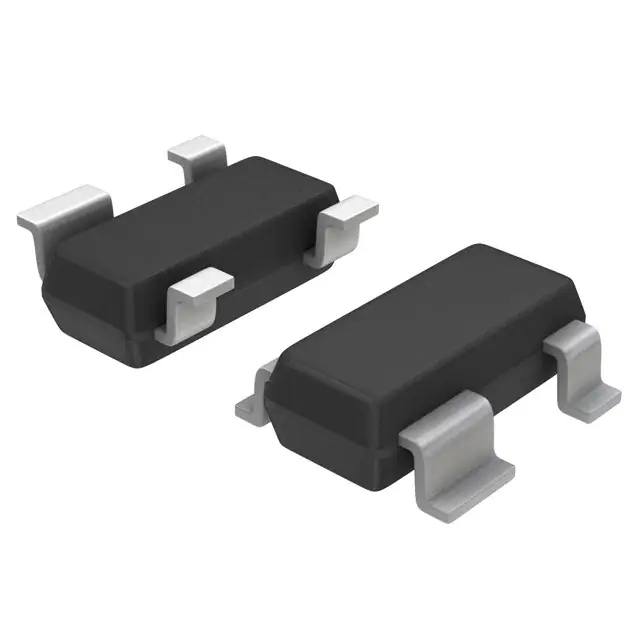
Package options for the MCP1754S include the SOT23A, SOT-89-3, SOT-223-3 and 2x3 DFN-8.
Package options for the MCP1754ST-3302E/CB include the SOT-23- 5, SOT-223-5, and 2x3 DFN-8.
Feature
- High PSRR: 72 dB @1 kHz Typical
- Low 56.0 µA Typical Quiescent Current
- Wide Input Operating Voltage Range: 3.6V to 16.0V
- 150 mA Output Current for All Output Voltages
- Low Drop Out Voltage, 300 mV Typical at 150 mA
- 0.4% Typical Output Voltage Regulation
- Standard Output Voltage Options (1.8V, 2.5V, 3.0V, 3.3V, 5.0V), Additional Options Available on Request
- Output Voltage Tolerances of ±2.0% Over Entire Temperature Range
- Stable with Minimum 1.0 µF Output Capacitance
- Power Good Output
- Shutdown Input
- True Current Foldback Protection
- Short-Circuit Protection
- Overtemperature Protection
- ESD protection (>4kV HBM)
(Picture:Pinout / Diagram)


