Component qualification in accordance with JEDEC and industry standards to ensure reliable operation over an extended temperature range. This includes, but is not limited to, Highly Accelerated Stress Test (HAST) or biased 85/85, temperature cycle, autoclave or unbiased HAST, electromigration, bond intermetallic life, and mold compound life. Such qualification testing should not be viewed as justifying use of this component beyond specified performance and environmental limits.
DescriptionThe UC2875SDWREP integrated circuit implements control of a bridge power stage by phase-shifting the switching of one half-bridge with respect to the other, allowing constant frequency pulse-width modulation in combination with resonant, zero-voltage switching for high efficiency performance at high frequencies. This circuit may be configured to provide control in either voltage or current mode operation, with a separate over-current shutdown for fast fault protection.
A programmable time delay is provided to insert a dead-time at the turn-on of each output stage. This delay, providing time to allow the resonant switching action, is independently controllable for each output pair (A-B, C-D).
With the oscillator capable of operation at frequencies in excess of 2 MHz, overall switching frequencies to 1 MHz are practical. In addition to the standard free running mode, with the CLOCKSYNC pin, the user may configure these devices to accept an external clock synchronization signal, or may lock together up to 5 units with the operational frequency determined by the fastest device.
Protective features include an undervoltage lockout which maintains all outputs in an active-low state until the supply reaches a 10.75 V threshold. 1.5 V hysteresis is built in for reliable, boot-strapped chip supply. Over-current protection is provided, and will latch the outputs in the OFF state within 70 ns of a fault. The current-fault circuitry implements full-cycle restart operation.
Additional features include an error amplifier with band-width in excess of 7 MHz, a 5 V reference, provisions for soft-starting, and flexible ramp generation and slope compensation circuitry.
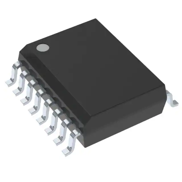
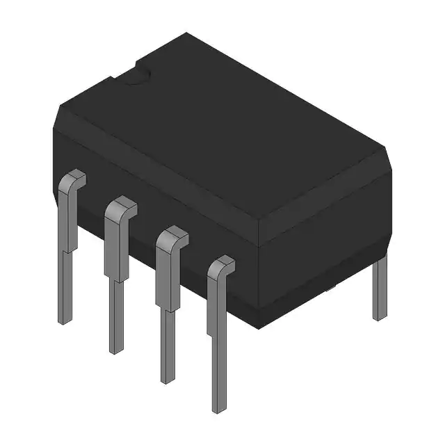
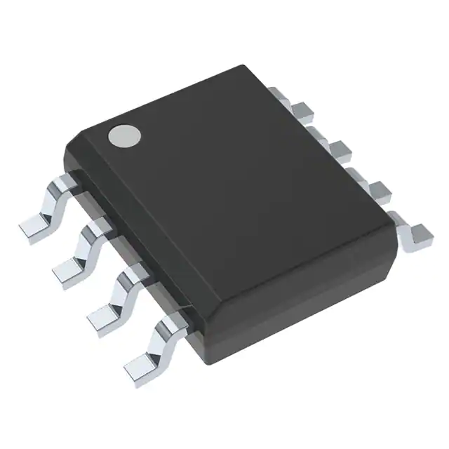
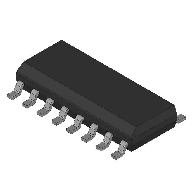
This device is available in 28-pin "bat-wing" SOIC plastic package for operation over –25°C to +110°C operation.
Feature
- Controlled Baseline
- One Assembly/Test Site, One Fabrication Site
- Extended Temperature Performance of –25°C to 110°C
- Enhanced Diminishing Manufacturing Sources (DMS) Support
- Enhanced Product Change Notification
- Qualification Pedigree
- Zero to 100% Duty Cycle Control
- Programmable Output Turn-On Delay
- Compatible with Voltage or Current Mode Topologies
- Practical Operation at Switching Frequencies to 1 MHz
- Four 2 A Totem Pole Outputs
- 10 MHz Error Amplifier
- Under-Voltage Lockout
- Low Startup Current –150 μA
- Outputs Active Low During UVLO
- Soft-Start Control
- Latched Over-Current Comparator With Full Cycle Restart
- Trimmed Reference
Component qualification in accordance with JEDEC and industry standards to ensure reliable operation over an extended temperature range. This includes, but is not limited to, Highly Accelerated Stress Test (HAST) or biased 85/85, temperature cycle, autoclave or unbiased HAST, electromigration, bond intermetallic life, and mold compound life. Such qualification testing should not be viewed as justifying use of this component beyond specified performance and environmental limits.
DescriptionThe UC2875 integrated circuit implements control of a bridge power stage by phase-shifting the switching of one half-bridge with respect to the other, allowing constant frequency pulse-width modulation in combination with resonant, zero-voltage switching for high efficiency performance at high frequencies. This circuit may be configured to provide control in either voltage or current mode operation, with a separate over-current shutdown for fast fault protection.
A programmable time delay is provided to insert a dead-time at the turn-on of each output stage. This delay, providing time to allow the resonant switching action, is independently controllable for each output pair (A-B, C-D).
With the oscillator capable of operation at frequencies in excess of 2 MHz, overall switching frequencies to 1 MHz are practical. In addition to the standard free running mode, with the CLOCKSYNC pin, the user may configure these devices to accept an external clock synchronization signal, or may lock together up to 5 units with the operational frequency determined by the fastest device.
Protective features include an undervoltage lockout which maintains all outputs in an active-low state until the supply reaches a 10.75 V threshold. 1.5 V hysteresis is built in for reliable, boot-strapped chip supply. Over-current protection is provided, and will latch the outputs in the OFF state within 70 ns of a fault. The current-fault circuitry implements full-cycle restart operation.
Additional features include an error amplifier with band-width in excess of 7 MHz, a 5 V reference, provisions for soft-starting, and flexible ramp generation and slope compensation circuitry.
This device is available in 28-pin "bat-wing" SOIC plastic package for operation over –25°C to +110°C operation.


