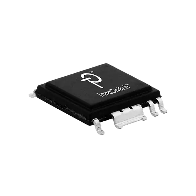
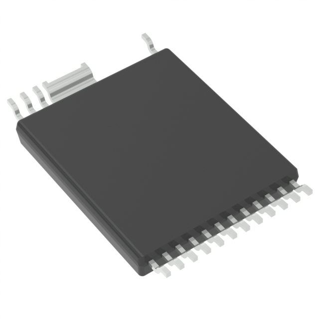
The InnoSwitch "-CH family of ICs dramatically simplifies the development and manufacturing of low-voltage, high current power supplies, particularly those in compact enclosures or with high efficiency requirements. The InnoSwitch-CH architecture is revolutionary in that the devices incorporate both primary and secondary controllers, with sense elements and a safety-rated feedback mechanism into a single IC.
Close component proximity and innovative use of the integratedcommunication link permit accurate control of a secondary-side synchronous rectification MOSFET and optimization of primary-side switching to maintain high efficiency across the entire load range.Additionally, the minimal DC bias requirements of the link enables thesystem to achieve less than 10 mW no-load in challenging applications such as smart-mobile device chargers.
Product Highlights
Highly Integrated, Compact Footprint
· Incorporates flyback controller,650 V MOSFET, secondary-side sensing and synchronous rectification driver
· Integrated FluxLink", HIPOT-isolated, feedback link
· Exceptional CV/CC accuracy, independent of transformer design or external components
· Instantaneous transient response ±5% CV with 0%-100%-0% load step
EcoSmart"-Energy Efficient
· <10 mW no-load at 230 VAC when supplied by transformer bias winding
· Easily meets all global energy efficiency regulations
· Low heat dissipation
Advanced Protection /Safety Features
· Primary sensed output OVP
· Secondary sensed output overshoot clamp
· Secondary sensed output OCP to zero output voltage
· Hysteretic thermal shutdown
Full Safety and Regulatory Compliance
·100% production HIPOT compliance testing equivalent to 6kV DC/1 sec
· Reinforced insulation
· Isolation voltage >3,500 VAC
· UL1577 and TUV(EN60950) safety approved
· EN61000-4-8(100 A/m) and EN61000-4-9(1000 A/m) compliant
Green Package
· Halogen free and RoHS compliant
Applications
· Chargers and adapters for smart mobile devices
· High efficiency, low voltage, high current power supplies
Feature
- Easily meets all global energy efficiency regulations
- Low heat dissipation
- Primary sensed output OVP
- Secondary sensed output overshoot clamp
- Secondary sensed output OCP to zero output voltage
- Hysteretic thermal shutdown
- Reinforced insulation
- Connection to external SR FET gate terminal
- Ground connection for the secondary IC
- Primary bypass pin regulator
- Primary bypass pin undervoltage threshold
- Primary bypass pin output overvoltage latching function
- Over temperature protection
- Current limit operation
- Auto-restart
- Safe-operating-area protection
- Primary-secondary handshake protocol
- Secondary controller
- Feedback pin auto-restart threshold
- Cable drop compensation
(Picture:Pinout / Diagram)

