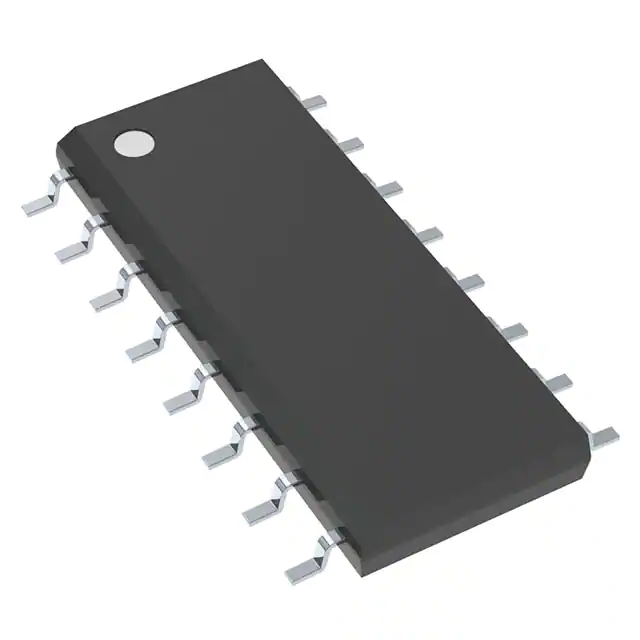
The MC14511BDR2G BCD-to-seven segment latch/decoder/driver is constructed with complementary MOS (CMOS) enhancement mode devices and NPN bipolar output drivers in a single monolithic structure. The circuit provides the functions of a 4-bit storage latch, an 8421 BCD-to-seven segment decoder, and an output drive capability. Lamp test (LTbar), blanking (BIbar), and latch enable (LE) inputs are used to test the display, to turn-off or pulse modulate the brightness of the display, and to store a BCD code, respectively. It can be used with seven-segment light-emitting diodes (LED), incandescent, fluorescent, gas discharge, or liquid crystal readouts either directly or indirectly. Applications include instrument (e.g., counter, DVM, etc.) display driver, computer/calculator display driver, cockpit display driver, and various clock, watch, and timer uses.
Feature
- Low Logic Circuit Power Dissipation
- High-Current Sourcing Outputs (Up to 25 mA)
- Latch Storage of Code
- Blanking Input
- Lamp Test Provision
- Readout Blanking on all Illegal Input Combinations
- Lamp Intensity Modulation Capability
- Time Share (Multiplexing) Facility
- Supply Voltage Range = 3.0 V to 18 V
- Capable of Driving Two Low-power TTL Loads, One Low-power Schottky TTL Load or Two HTL Loads Over the Rated Temperature Range
- Chip Complexity: 216 FETs or 54 Equivalent Gates
- Triple Diode Protection on all Inputs
- These devices are available in Pb-free package(s). Specifications herein apply to both standard and Pb-free devices. Please see our website at www.onsemi.com for specific Pb-free orderable part numbers, or contact your local ON Semiconductor sales office or representative.
(Picture: Pinout)


