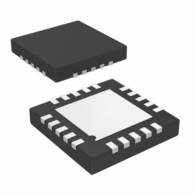
The ADP5063ACPZ-1-R7 operates from a 4 V to 6.7 V input voltage range but is tolerant of voltages up to 20 V, thereby alleviating concerns about USB bus spikes during disconnection or connection scenarios.
The ADP5063ACPZ-1-R7 features an internal field effect transistor (FET) between the linear charger output and the battery. This permits battery isolation and, therefore, system powering under a dead battery or no battery scenario, which allows immediate system function upon connection to a USB power supply.
Based on the type of USB source, which is detected by an external USB detection chip, the ADP5063ACPZ-1-R7 can be set to apply the correct current limit for optimal charging and USB compliance.
The ADP5063ACPZ-1-R7 has three factory-programmable digital input/out-put pins that provide maximum flexibility for different systems. These digital input/output pins permit a combination of features, such as input current limits, charging enable and disable, charging current limits, and a dedicated interrupt output pin.
Feature
- Default charging termination voltage at 3.6 V
- Fully compatible with USB 3.0 and USB Battery Charging 1.2 Compliance Plan Specification
- Operating input voltage from 4 V to 6.7 V
- Tolerant input voltage from −0.5 V to +20 V (USB VBUS)
- Fully programmable via I2C
- Flexible digital control inputs
- Up to 2.1 A current from an ac charger in LDO mode
- Built-in current sensing and limiting
- As low as 55 mΩ battery isolation FET between battery and charger output
- Thermal regulation prevents overheating
- Compliant with JEITA 1 and JEITA 2 Li-Ion battery charging temperature specifications
- SYS_EN flag permits the system to be disabled until battery is at the minimum required level for guaranteed system start-up
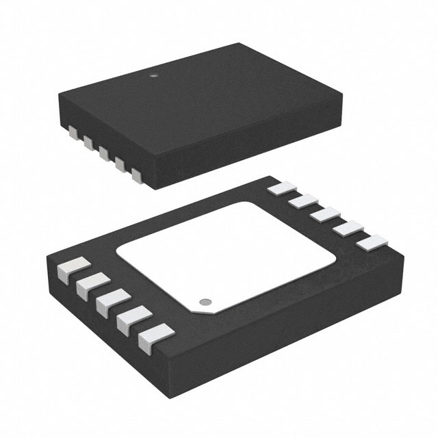
- 4 mm × 4 mm LFCSP package
Applications
- Single cell LiFePO4 portable equipment
- Portable medical devices
- Portable instrumentation devices
- Portable consumer devices
(Picture: Pinout)

