The XC6501B181GR-G series is a 6.0V high speed, low noise CMOS LDO regulator that can provide stable output voltages within a range of 1.2V to 5.0V (0.05V increments) even without a load capacitor CL. This is possible because phase compensation is carried out internally unlike other LDOs where it is done externally. The series consists of a reference voltage source, driver transistor, error amplifier, current limit circuit, and phase compensation circuit. The CE function enables the circuit to be put into stand-by mode by inputting a low level signal to the CE pin thereby reducing current consumption from an already low 13?A (in operation) to less than 0.1?A. In the stand-by mode, if a CL cap is used, the electric charge stored at CL can be discharged via the internal auto-discharge switch and as a result, the VOUT pin quickly returns to the VSS level. The current limit fold-back circuit operates as a short circuit protection and a current limiter function for the output pin.
Feature
■
Operating Voltage Range : 1.4~6.0V
Output Voltage Range : 2.0~5.0V(Accuracy:±1%)
1.2~1.95V(Accuracy:±0.02V)
Dropout Voltage : 150mV@IOUT=100mA, VOUT=2.8V
Low Power Supply : 13μA@VOUT=2.8V
Stand-by Current : Less than 0.1μA
Ripple Rejection : 50dB@f=1kHz,VOUT=2.8V
Protection Circuits : Current limit (300mA, TYP.)
: Short circuit protection
Output capacitor is not required : Internal phase compensation
CL High Speed Auto Discharge
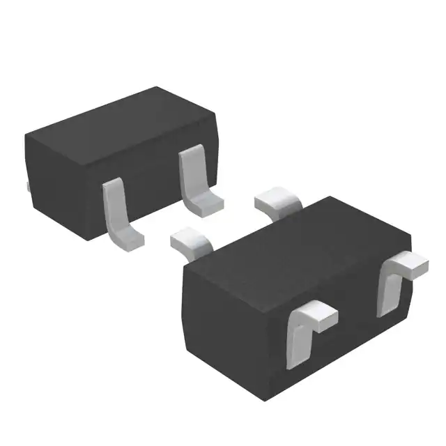
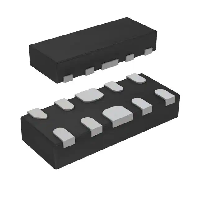
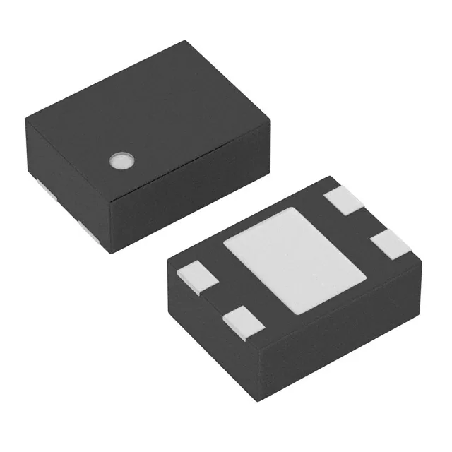
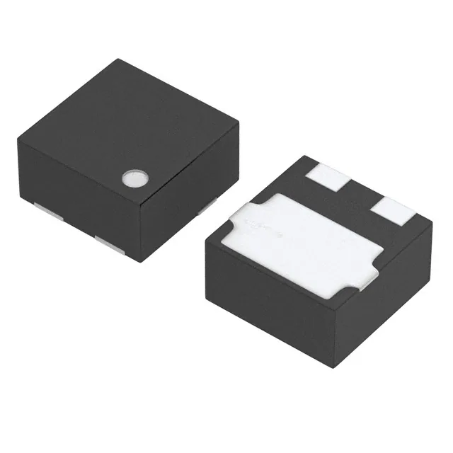
Packages USP-3, USP-4
SSOT-24, SOT-25


