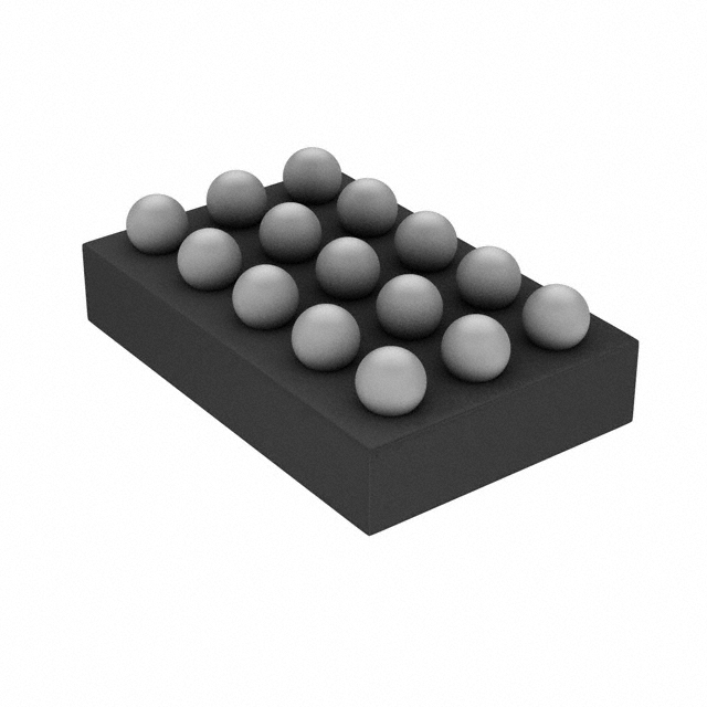
The TPS65132BYFFR family is designed to supply positive/negative driven applications. The device uses a single inductor scheme for both outputs to provide the user smallest solution size, a small bill-of-material as well as high efficiency. The devices offer best line and load regulation at low noise. With its input voltage range of 2.5 V to 5.5 V, it is optimized for products powered by single-cell batteries (Li-Ion, Ni-Li, Li-Polymer) and fixed 3.3-V and 5-V rails. The TPS656132 family provides 80 mA and 150 mA output current options with programmability to 40 mA. There are both CSP and QFN package options available.
Feature
- Input Voltage Range: 2.5 V to 5.5 V
- VPOS Boost Converter: 4 V to 6 V (0.1-V step)
- VNEG Inverting Buck-Boost Converter: –6 V to –4 V (0.1-V step)
- Maximum Output Current: 80 mA or 150 mA
- Outstanding Combined Efficiency
- > 85% at IOUT > 10 mA
- > 90% at IOUT > 40 mA
- Excellent Performance
- Outstanding Transient Response
- 1% Output Voltage Accuracy over Full Temperature Range
- I2C Interface
- Programmable Power-Up / -Down Sequencing Options
- Flexible Output Voltage Programming
- Programmable Active Output Discharge
- > 1000x Programmable Non-Volatile Memory
- Under-Voltage Lock-Out and Thermal Protection
- Two Package Options
- 15-Ball CSP Package
- 20-Pins QFN Package
The TPS65132 family is designed to supply positive/negative driven applications. The device uses a single inductor scheme for both outputs to provide the user smallest solution size, a small bill-of-material as well as high efficiency. The devices offer best line and load regulation at low noise. With its input voltage range of 2.5 V to 5.5 V, it is optimized for products powered by single-cell batteries (Li-Ion, Ni-Li, Li-Polymer) and fixed 3.3-V and 5-V rails. The TPS656132 family provides 80 mA and 150 mA output current options with programmability to 40 mA. There are both CSP and QFN package options available.


