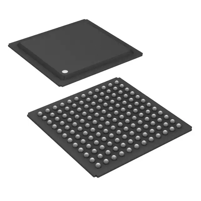
The AD9172BBPZRL is a high performance, dual, 16-bit digital-to-analog converter (DAC) that supports DAC sample rates to 12.6 GSPS. The device features an 8-lane, 15 Gbps JESD204B data input port, a high performance, on-chip DAC clock multiplier, and digital signal processing capabilities targeted at single-band and multiband direct to radio frequency (RF) wireless applications.
The AD9172BBPZRL features three complex data input channels per RF DAC that are bypassable. Each data input channel includes a configurable gain stage, an interpolation filter, and a channel numerically controlled oscillator (NCO) for flexible, multiband frequency planning. The device supports up to a 1.5 GSPS complex data rate per input channel and is capable of aggregating multiple complex input data streams up to a maximum complex data rate of 1.5 GSPS. Additionally, the AD9172BBPZRL supports ultrawide bandwidth modes bypassing the channelizers to provide maximum data rates of up to 3.08 GSPS (with 16-bit resolution) and 4.1 GSPS (with 12-bit resolution).
The AD9172BBPZRL is available in a 144-ball BGA_ED package.
Product Highlights
Feature
- Supports multiband wireless applications
- 3 bypassable, complex data input channels per RF DAC
- 1.54 GSPS maximum complex input data rate per input channel
- 1 independent NCO per input channel
- Proprietary, low spurious and distortion design
- 2-tone intermodulation distortion (IMD) = −83 dBc at 1.8 GHz, −7 dBFS/tone RF output
- Spurious free dynamic range (SFDR) <−80 dBc at 1.8 GHz, −7 dBFS RF output
- Flexible 8-lane, 15.4 Gbps JESD204B interface
- Supports single-band and multiband use cases
- Supports 12-bit high density mode for increased data throughput
- Multiple chip synchronization
- Supports JESD204B Subclass 1
- Selectable interpolation filter for a complete set of input data rates
- 1×, 2×, 3×, 4×, 6×, and 8× configurable data channel interpolation
- 1×, 2×, 4×, 6×, 8×, and 12× configurable final interpolation
- Final 48-bit NCO that operates at the DAC rate to support frequency synthesis up to 6 GHz
- Transmit enable function allows extra power saving and downstream circuitry protection
- High performance, low noise PLL clock multiplier
- Supports 12.6 GSPS DAC update rate
- Observation ADC clock driver with selectable divide ratios
- Low power
- 2.55 W at 12 GSPS, dual channel mode
- 10 mm × 10 mm, 144-ball BGA_ED with metal enhanced thermal lid, 0.80 mm pitch
Applications
- Wireless communications infrastructure
- Multiband base station radios
- Microwave/E-band backhaul systems
- Instrumentation, automatic test equipment (ATE)
- Radars and jammers
(Picture: Pinout)


