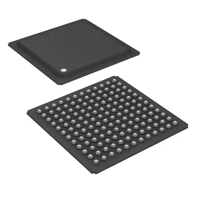
The AD9176BBPZRL is a high performance, dual, 16-bit digital-to-analog converter (DAC) that supports DAC sample rates up to 12.6 GSPS. The device features an 8-lane, 15.4 Gbps JESD204B data input port, a high performance, on-chip DAC clock multiplier, and digital signal processing capabilities targeted at single-band and multiband direct to radio frequency (RF) wireless applications.
The AD9176BBPZRL features three complex data input channels per RF DAC datapath. Each input channel is fully bypassable. Each data input channel (or channelizer) includes a configurable gain stage, an interpolation filter, and a channel numerically controlled oscillator (NCO) for flexible, multiband frequency planning. The AD9176BBPZRL supports an input data rate of up to a 3.08 GSPS complex (inphase/quadrature (I/Q)), or up to 6.16 GSPS non-complex (real), and is capable of allocating multiple complex input data streams to the assigned channels for individual processing. Each group of three channelizers is summed into a respective main datapath for additional processing when needed. Each main datapath includes an interpolation filter and one 48-bit main NCO ahead of the RF DAC core. Using the modulator switch, the outputs of a main datapath can be either routed to DAC0 alone for operating as a single DAC, or routed to both DAC0 and DAC1 for operating as a dual, intermediate frequency DAC (IF DAC).
The AD9176BBPZRL also supports ultrawide data rate modes that allow bypassing the channelizers and main datapaths to provide maximum data rates of up to 6.16 GSPS as a single, 16-bit DAC, up to 3.08 GSPS as a dual, 16-bit DAC, or up to 4.1 GSPS as a dual, 12-bit DAC.
The AD9176BBPZRL is available in a 144-ball BGA_ED package.
Feature
- Supports multiband wireless applications
- 3 bypassable, complex data input channels per RF DAC
- 3.08 GSPS maximum complex input data rate per input channel
- 1 independent NCO per input channel
- Proprietary, low spurious and distortion design
- 2-tone IMD3 = −83 dBc at 1.84GHz, −7 dBFS/tone RF output
- SFDR <−80 dBc at 1.84 GHz, −7 dBFS RF output
- Flexible 8-lane, 15.4 Gbps JESD204B interface
- Supports single-band and multiband use cases
- Supports 12-bit high density mode for increased data throughput
- Multiple chip synchronization
- Supports JESD204B Subclass 1
- Selectable interpolation filter for a complete set of input data rates
- 1×, 2×, 3×, 4×, 6×, and 8× configurable data channel interpolation
- 1×, 2×, 4×, 6×, 8×, and 12× configurable final interpolation
- Final 48-bit NCO that operates at the DAC rate to support frequency synthesis up to 6 GHz
- Transmit enable function allows extra power saving and downstream circuitry protection
- High performance, low noise PLL clock multiplier
- Supports 12.6 GSPS DAC update rate
- Observation ADC clock driver with selectable divide ratios
- Low power
- 2.54 W with 2 DACs at 12 GSPS, DAC PLL on
- 10 mm × 10 mm, 144-ball BGA_ED with metal enhanced thermal lid, 0.80 mm pitch
Applications
- Wireless communications infrastructure
- Multiband base station radios
- Microwave/E-band backhaul systems
- Instrumentation, automatic test equipment (ATE)
- Radars and jammers
Product Highlights
(Picture: Pinout)


