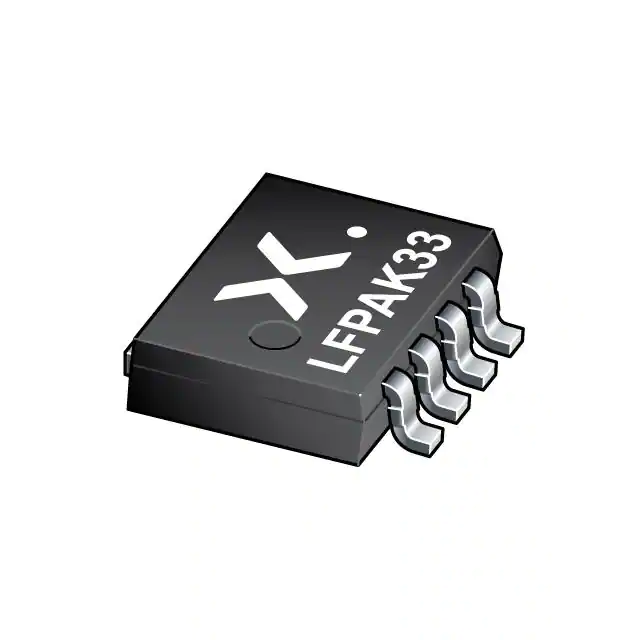
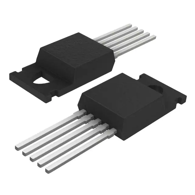
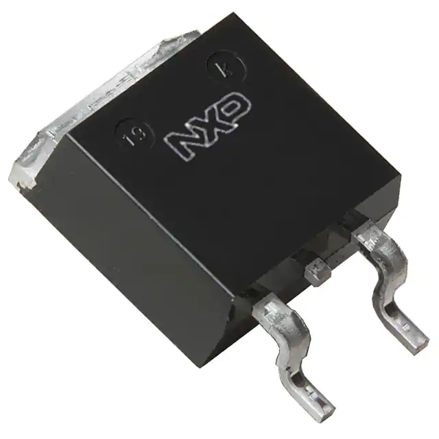
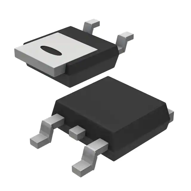
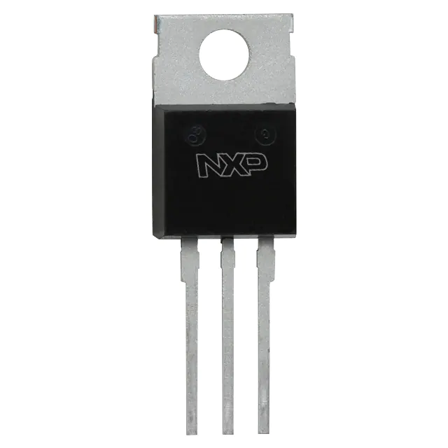
The BUK7Y7R2-60E,115 parts manufactured by NEXPERIA are available for purchase at 9icnet Electronics. Here you can find various types and values of electronic parts from the world's leading manufacturers. The BUK7Y7R2-60E,115 components of 9icnet Electronics are carefully chosen, undergo stringent quality control, and are successfully meet all required standards.
The production status marked on 9icnet.com is for reference only. If you didn't find what you were looking for, you can get more valuable information by emails, such as the BUK7Y7R2-60E,115 Inventory quantity, preferential price, datasheet, and manufacturer. We are always happy to hear from you, so feel free to contact us.
BUK7Y59-60EX with pin details, that includes Reel Packaging, they are designed to operate with a BUK7Y59-60E115 Part Aliases, Mounting Style is shown on datasheet note for use in a SMD/SMT, that offers Package Case features such as LFPAK-4, Technology is designed to work in Si, as well as the 1 Channel Number of Channels, the device can also be used as Single Configuration. In addition, the Transistor Type is 1 N-Channel, the device is offered in 37 W Pd Power Dissipation, it has an Maximum Operating Temperature range of + 175 C, it has an Minimum Operating Temperature range of - 55 C, and the Fall Time is 5.2 ns, and Rise Time is 5.5 ns, and the Vgs Gate Source Voltage is 20 V, and Id Continuous Drain Current is 17 A, and the Vds Drain Source Breakdown Voltage is 60 V, and Vgs th Gate Source Threshold Voltage is 3 V, and the Rds On Drain Source Resistance is 38.2 mOhms, and Transistor Polarity is N-Channel, and the Typical Turn Off Delay Time is 6.5 ns, and Typical Turn On Delay Time is 3.8 ns, and the Qg Gate Charge is 7.8 nC, and Channel Mode is Enhancement.
BUK7Y65-100EX with user guide, that includes 3 V Vgs th Gate Source Threshold Voltage, they are designed to operate with a 20 V Vgs Gate Source Voltage, Vds Drain Source Breakdown Voltage is shown on datasheet note for use in a 100 V, that offers Typical Turn On Delay Time features such as 5.3 ns, Typical Turn Off Delay Time is designed to work in 12.4 ns, as well as the 1 N-Channel Transistor Type, the device can also be used as N-Channel Transistor Polarity. In addition, the Technology is Si, the device is offered in 7.5 ns Rise Time, the device has a 44 mOhms of Rds On Drain Source Resistance, and Qg Gate Charge is 17.8 nC, and the Pd Power Dissipation is 64 W, and Packaging is Reel, and the Package Case is LFPAK-4, and Number of Channels is 1 Channel, and the Mounting Style is SMD/SMT, it has an Minimum Operating Temperature range of - 55 C, it has an Maximum Operating Temperature range of + 175 C, and Id Continuous Drain Current is 19 A, and the Fall Time is 8 ns, and Configuration is Single, and the Channel Mode is Enhancement.
BUK7Y6R0-60EX with circuit diagram, that includes Enhancement Channel Mode, they are designed to operate with a Single Configuration, Fall Time is shown on datasheet note for use in a 21 ns, that offers Id Continuous Drain Current features such as 100 A, it has an Maximum Operating Temperature range of + 175 C, it has an Minimum Operating Temperature range of - 55 C, the device can also be used as SMD/SMT Mounting Style. In addition, the Number of Channels is 1 Channel, the device is offered in LFPAK-4 Package Case, the device has a Reel of Packaging, and Pd Power Dissipation is 195 W, and the Qg Gate Charge is 45.4 nC, and Rds On Drain Source Resistance is 4 mOhms, and the Rise Time is 19 ns, and Technology is Si, and the Transistor Polarity is N-Channel, and Transistor Type is 1 N-Channel, and the Typical Turn Off Delay Time is 36 ns, and Typical Turn On Delay Time is 12 ns, and the Vds Drain Source Breakdown Voltage is 60 V, and Vgs Gate Source Voltage is 20 V, and the Vgs th Gate Source Threshold Voltage is 3 V.
BUK7Y72-80EX with EDA / CAD Models, that includes SMD/SMT Mounting Style, they are designed to operate with a Single Configuration, Technology is shown on datasheet note for use in a Si, that offers Packaging features such as Reel, Transistor Polarity is designed to work in N-Channel, as well as the LFPAK-4 Package Case, the device can also be used as Enhancement Channel Mode. In addition, the Qg Gate Charge is 9.8 nC, the device is offered in 80 V Vds Drain Source Breakdown Voltage, the device has a 8 ns of Typical Turn Off Delay Time, and Rds On Drain Source Resistance is 72 mOhms, and the Fall Time is 5 ns, and Pd Power Dissipation is 45 W, and the Rise Time is 4 ns, and Typical Turn On Delay Time is 4 ns, and the Vgs th Gate Source Threshold Voltage is 3 V, and Vgs Gate Source Voltage is 20 V, and the Id Continuous Drain Current is 16 A, and Transistor Type is 1 N-Channel, and the Number of Channels is 1 Channel, it has an Maximum Operating Temperature range of + 175 C, it has an Minimum Operating Temperature range of - 55 C.

