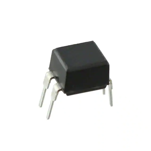
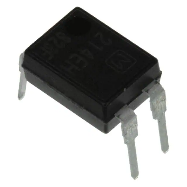
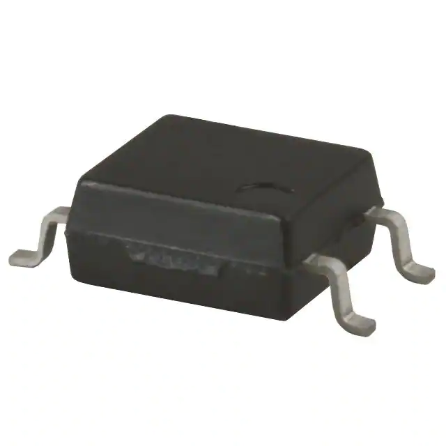
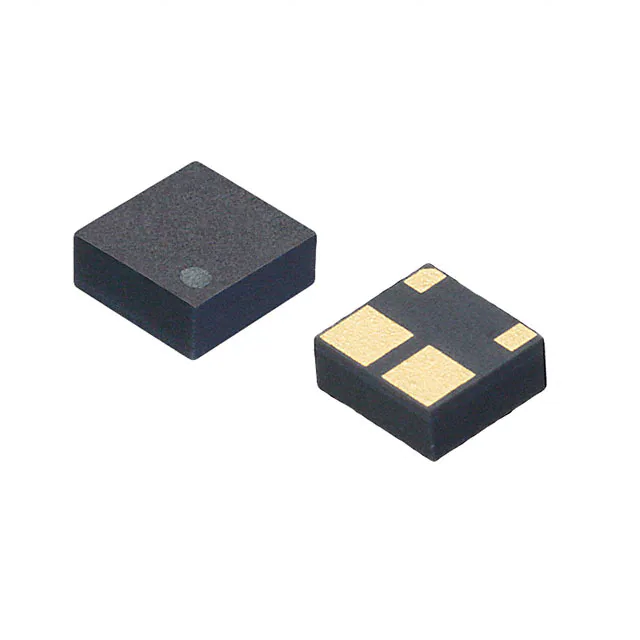
FEATURES
1. High cost-performance type of PhotoMOS 1 Form B output
2. Low on-resistance This has been realized thanks to the built-in MOSFET processed by our proprietary method, DSD(Double-
diffused and Selective Doping) method.
3. Reinforced insulation of 5,000V More than 0.4 mm internal insulationdistance between inputs and outputs.
Conforms to EN41003, EN60950
(reinforced insulation).
4. Controls low-level analog signals PhotoMOS feature extremely low closed-
circuit offset voltage to enable control of low-level analog signals without distortion.
5. High sensitivity and low on-
resistance Can control max.0.55 A load current with
5 mA input current.
Low on-resistance of typ.1Ω
(AQY412EH).
6. Low-level off-state leakage current
TYPICAL APPLICATIONS
·Power supply
·Measuring equipment
·Security equipment
·Modem
·Telephone equipment
·Electricity,plant equipment
·Sensing equipment
(Picture:Pinout / Diagram)

