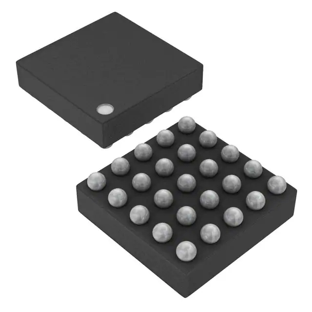
The LTM®4632 is an ultrathin triple output step-down µModule® (power module) regulator to provide complete power solution for DDR-QDR4 SRAM. Operating from a 3.6V to 15V input voltage, the LTM4632IV#PBF supports two ±3A output rails, both sink and source capable, for VDDQ and VTT, plus a 10mA low noise reference VTTR output. Both VTT and VTTR track and are equal to VDDQ/2. Housed in a 6.25mm × 6.25mm × 1.82mm LGA and 6.25mm × 6.25mm × 2.42mm BGA packages, the LTM4632IV#PBF includes the switching controller, power FETs, inductors and support components. Alternatively, the power module can also be configured as a two phase single ±6A output VTT. Only a few ceramic input and output capacitors are needed to complete the design.
The LTM4632IV#PBF supports selectable Burst Mode operation (CH1 only) and output voltage tracking for supply rail sequencing. Its high switching frequency and current mode control enable a very fast transient response to line and load changes without sacrificing stability.
Fault protection features include overvoltage input, overcurrent and overtemperature protection.
The LTM4632IV#PBF is available with SnPb (BGA) or RoHS compliant terminal finish
FEATURES
• Complete DDR-QDR4 SRAM Power Solution Including VDDQ, VTT, VTTR (or VREF)
• Solution in 0.5cm2 (Dual-Sided PCB)
• Wide Input Voltage Range: 3.6V to 15V
• 3.3V Input Compatible with VIN Tied to INTVCC
• 0.6V to 2.5V Output Voltage Range
• Dual ±3A DC Output Current with Sink and Source Capability
• ±1.5%, ±10mA Buffered VTTR = VDDQ/2 Output
• 3A VDDQ + 3A VTT or Dual Phase Single 6A VTT
• ±1.5% Maximum Total Output Voltage Regulation Error Over Load, Line and Temperature
• Current Mode Control, Fast Transient Response
• External Frequency Synchronization
• Multiphase Parallelable with Current Sharing
• Selectable Burst Mode® Operation
• Overvoltage Input and Overtemperature Protection
• Power Good Indicator
• Ultrathin 6.25mm × 6.25mm × 1.82mm LGA and 6.25mm × 6.25mm × 2.42mm BGA Packages
APPLICATIONS
• DDR Memory Power Supply
• General Purpose Point-of-Load Conversion
• Telecom, Networking and Industrial Equipment
Feature
- Complete DDR-QDR4 SRAM Power Solution Including VDDQ, VTT, VTTR (or VREF)
- Solution in 0.5cm2 (Dual-Sided PCB)
- Wide Input Voltage Range: 3.6V to 15V
- 3.3V Input Compatible with VIN Tied to INTVCC
- 0.6V to 2.5V Output Voltage Range
- Dual ±3A DC Output Current with Sink and Source Capability
- ±1.5%, ±10mA Buffered VTTR = VDDQ/2 Output
- 3A VDDQ + 3A VTT or Dual Phase Single 6A VTT
- ±1.5% Maximum Total Output Voltage Regulation Error Over Load, Line and Temperature
- Current Mode Control, Fast Transient Response
- External Frequency Synchronization
- Multiphase Parallelable with Current Sharing
- Selectable Burst Mode® Operation
- Overvoltage Input and Overtemperature Protection
- Power Good Indicator
- Ultrathin 6.25mm × 6.25mm × 1.82mm LGA and 6.25mm × 6.25mm × 2.42mm BGA Packages
Applications
- DDR Memory Power Supply
- General Purpose Point of Load Conversion
- Telecom, Networking and Industrial Equipment
(Picture:Pinout / Diagram)


