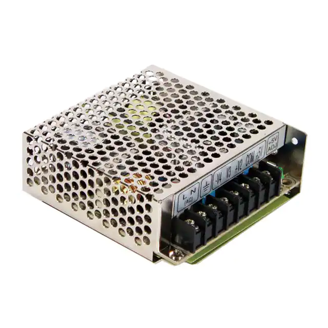
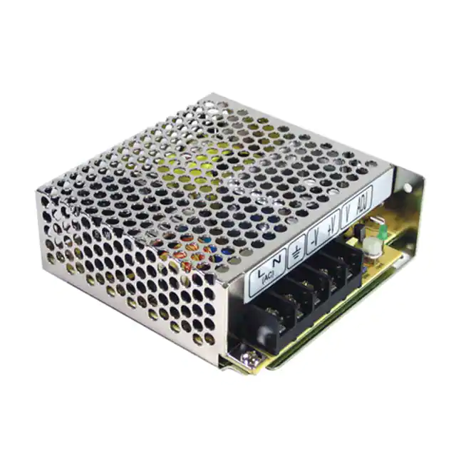
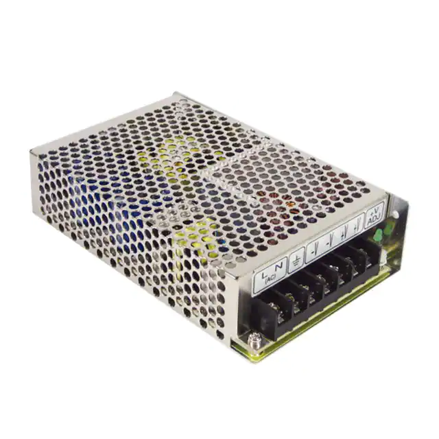
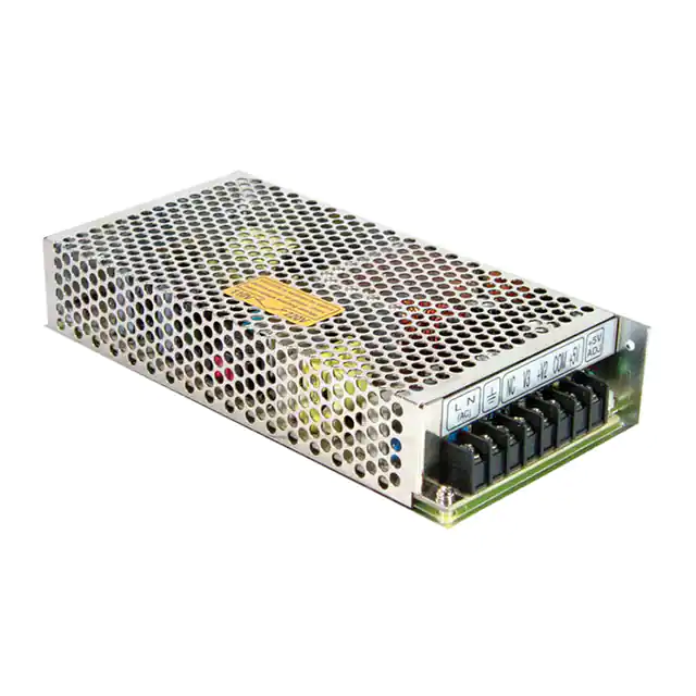
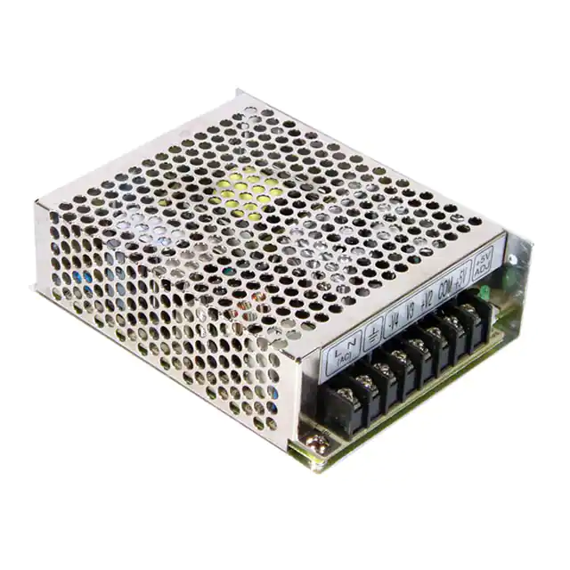
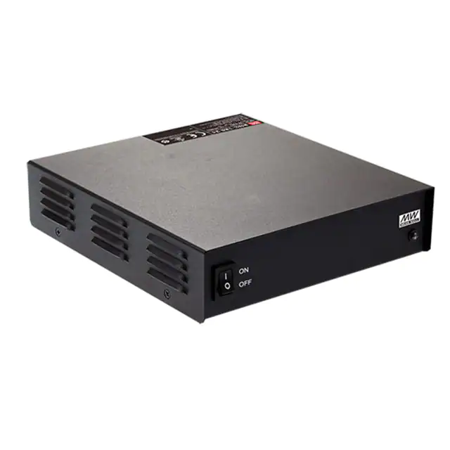
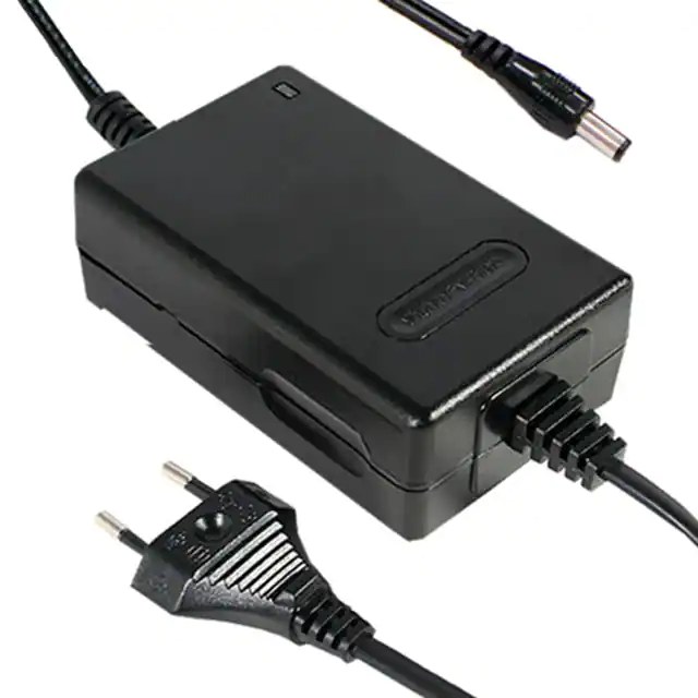
The RQ-85B parts manufactured by MEAN WELL are available for purchase at 9icnet Electronics. Here you can find various types and values of electronic parts from the world's leading manufacturers. The RQ-85B components of 9icnet Electronics are carefully chosen, undergo stringent quality control, and are successfully meet all required standards.
The production status marked on 9icnet.com is for reference only. If you didn't find what you were looking for, you can get more valuable information by emails, such as the RQ-85B Inventory quantity, preferential price, datasheet, and manufacturer. We are always happy to hear from you, so feel free to contact us.
RQ6E050ATTCR with pin details, that includes RQ6E050AT Series, they are designed to operate with a Digi-ReelR Alternate Packaging Packaging, Mounting Style is shown on datasheet note for use in a SMD/SMT, that offers Package Case features such as SC-74, SOT-457, Technology is designed to work in Si, it has an Operating Temperature range of 150°C (TJ), the device can also be used as Surface Mount Mounting Type. In addition, the Number of Channels is 1 Channel, the device is offered in TSMT6 Supplier Device Package, the device has a 1 P-Channel of Configuration, and FET Type is MOSFET P-Channel, Metal Oxide, and the Power Max is 1.25W, and Transistor Type is 1 P-Channel, and the Drain to Source Voltage Vdss is 30V, and Input Capacitance Ciss Vds is 940pF @ 15V, and the FET Feature is Standard, and Current Continuous Drain Id 25°C is 5A (Ta), and the Rds On Max Id Vgs is 27 mOhm @ 5A, 10V, and Vgs th Max Id is 2.5V @ 1mA, and the Gate Charge Qg Vgs is 20.8nC @ 10V, and Pd Power Dissipation is 1.25 W, it has an Maximum Operating Temperature range of + 150 C, it has an Minimum Operating Temperature range of - 55 C, and the Fall Time is 22 ns, and Rise Time is 16 ns, and the Vgs Gate Source Voltage is +/- 20 V, and Id Continuous Drain Current is +/- 5 A, and the Vds Drain Source Breakdown Voltage is - 30 V, and Vgs th Gate Source Threshold Voltage is - 2.5 V, and the Rds On Drain Source Resistance is 38 mOhms, and Transistor Polarity is P-Channel, and the Typical Turn Off Delay Time is 55 ns, and Typical Turn On Delay Time is 9.6 ns, and the Qg Gate Charge is 20.8 nC, and Channel Mode is Enhancement.
RQ6P015SPTR with user guide, that includes RQ6P015SP Series, they are designed to operate with a Reel Packaging.
RQ6E055BNTCR with circuit diagram, that includes Reel Packaging, they are designed to operate with a Si Technology.


