Feature
Overview:
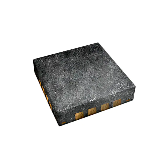
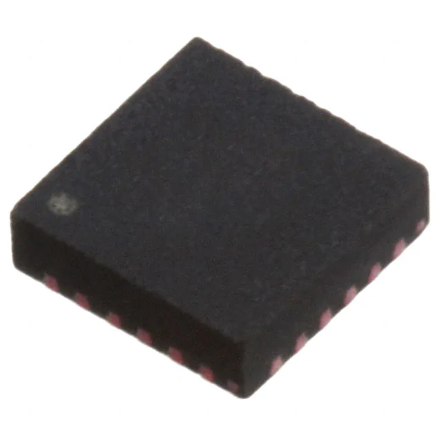
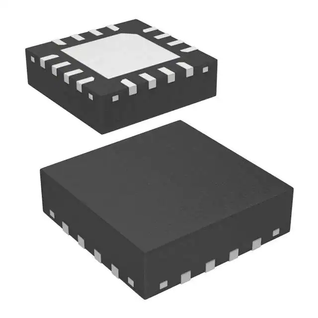
The ITG-1010 is a single-chip, digital output, 3 Axis MEMS gyroscope IC which features a 512-byte FIFO. The FIFO can lower the traffic on the serial bus interface, and reduce power consumption by allowing the system processor to burst read sensor data and then go into a low-power mode. The gyroscope includes a programmable full-scale range of ±250, ±500, ±1000, and ±2000 degrees/sec, very low Rate noise at 0.01 dps/√Hz and extremely low power consumption at 3.2mA. Factory-calibrated initial sensitivity reduces production-line calibration requirements. Other industry-leading features include on-chip 16-bit ADCs, programmable digital filters, a precision clock with 1% drift from -40°C to 85°C, an embedded temperature sensor, and programmable interrupts. The device features I 2 C and SPI serial interfaces, a VDD operating range of 1.71 to 3.6V, and a separate digital IO supply, VDDIO from 1.71V to 3.6V. By leveraging its patented and volume-proven CMOS-MEMS fabrication platform, which integrates MEMS wafers with companion CMOS electronics through wafer-level bonding, InvenSense has driven the gyro package size down to a footprint and thickness of 3x3x0.9mm (16-pin QFN), to provide a very small yet high performance low cost package. The device provides high robustness by supporting 10,000g shock reliability.
Applications:
• Motion UI
• Handset gaming
• Location based services, points of interest, and dead reckoning
• Health and sports monitoring
• Power management
Features:
The ITG-1010 MEMS gyroscope includes a wide range of features:
Sensors:
• Monolithic X-, Y-, Z-Axis angular rate sensor (gyros) integrated circuit
• Digital-output temperature sensor
• External sync signal connected to the FSYNC pin supports image, video and GPS
synchronization
• Factory calibrated scale factor
• High cross-axis isolation via proprietary MEMS design
• 10,000g shock tolerant
Digital Output:
• The total data set obtained by the device includes gyroscope data, temperature data, and the one
bit external sync signal connected to the FSYNC pin.
• FIFO allows burst read, reduces serial bus traffic and saves power on the system processor.
• FIFO can be accessed through both I2
C and SPI interfaces.
• Programmable interrupt
• Programmable low-pass filters
Clocking:
• On-chip timing generator clock frequency ±1% drift over full temperature range
Power:
• VDD supply voltage range of 1.71V to 3.6V
• Flexible VDDIO reference voltage allows for multiple I2
C and SPI interface voltage levels
• Power consumption with three axes active: 3.2mA
• Sleep mode: 8μA
• Each axis can be individually powered down
Package:
• 3x3x0.9mm footprint and maximum thickness 16-pin QFN plastic package
• MEMS structure hermetically sealed at wafer level
• RoHS and Green compliant
(Picture:Pinout / Diagram)


