The AD7887BR-REEL7 can be configured for either dual- or single-channel operation via the on-chip control register. There is a default single-channel mode that allows the AD7887BR-REEL7 to be operated as a read-only ADC. In single-channel operation, there is one analog input (AIN0) and the AIN1/VREF pin assumes its VREF function. This VREF pin allows the user access to the part’s internal 2.5 V reference, or the VREF pin can be overdriven by an external reference to provide the reference voltage for the part. This external reference voltage has a range of 2.5 V to VDD. The analog input range on AIN0 is 0 to VREF.
In dual-channel operation, the AIN1/VREF pin assumes its AIN1 function, providing a second analog input channel. In this case, the reference voltage for the part is provided via the VDD pin. As a result, the input voltage range on both the AIN0 and AIN1 inputs is 0 to VDD.
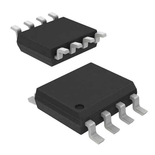
CMOS construction ensures low power dissipation of typically 2 mW for normal operation and 3 μW in power-down mode. The part is available in an 8-lead, 0.15-inch-wide narrow body SOIC and an 8-lead MSOP package.
Product HighlightsFeature
- Specified for VDD of 2.7 V to 5.25 V
- Flexible power/throughput rate management
- Shutdown mode: 1 μA max
- One or two single-ended inputs
- Serial interface: SPI®/QSPI™/MICROWIRE™/DSP compatible
- 8-lead narrow SOIC and MSOP packages
Applications
- Battery-powered systems (personal digital assistants, medical instruments, mobile communications)
- Instrumentation and control systems
- High speed modems
(Picture: Pinout)


