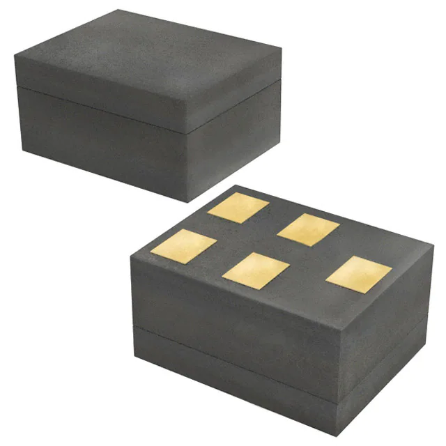
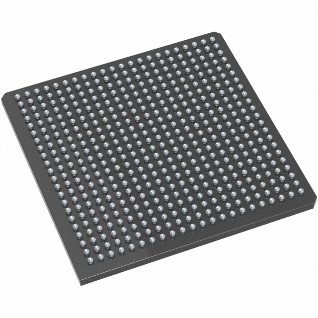
The Fusion mixed signal FPGA satisfies the demand from system architects for a device that simplifies design and unleashes their creativity. As the world’s first mixed signal programmable logic family, Fusion integrates mixed signal analog, flash memory, and FPGA fabric in a monolithic device. Fusion devices enable designers to quickly move from concept to completed design and then deliver feature-rich systems to market. This new technology takes advantage of the unique properties of Microsemi flash-based FPGAs, including a high-isolation, triple-well process and the ability to support high-voltage transistors to meet the demanding requirements of mixed signal system design.
Fusion mixed signal FPGAs bring the benefits of programmable logic to many application areas, including power management, smart battery charging, clock generation and management, and motor control. Until now, these applications have only been implemented with costly and space-consuming discrete analog components or mixed signal ASIC solutions. Fusion mixed signal FPGAs present new capabilities for system development by allowing designers to integrate a wide range of functionality into a single device, while at the same time offering the flexibility of upgrades late in the manufacturing process or after the device is in the field. Fusion devices provide an excellent alternative to costly and time-consuming mixed signal ASIC designs. In addition, when used in conjunction with the ARM Cortex-M1 processor, Fusion technology represents the definitive mixed signal FPGA platform.
Feature
• Advanced 130-nm, 7-Layer Metal, Flash-Based CMOS Process
• Nonvolatile, Retains Program when Powered Off
• Instant On Single-Chip Solution
• 350 MHz System Performance
Embedded Flash Memory
• User Flash Memory – 2 Mbits to 8 Mbits
– Configurable 8-, 16-, or 32-Bit Datapath
– 10 ns Access in Read-Ahead Mode
• 1 Kbit of Additional FlashROM
Integrated A/D Converter (ADC) and Analog I/O
• Up to 12-Bit Resolution and up to 600 Ksps
• Internal 2.56 V or External Reference Voltage
• ADC: Up to 30 Scalable Analog Input Channels
• High-Voltage Input Tolerance: –10.5 V to +12 V
• Current Monitor and Temperature Monitor Blocks
• Up to 10 MOSFET Gate Driver Outputs
– P- and N-Channel Power MOSFET Support
– Programmable 1, 3, 10, 30 µA, and 20 mA Drive Strengths
• ADC Accuracy is Better than 1%
On-Chip Clocking Support
• Internal 100 MHz RC Oscillator (accurate to 1%)
• Crystal Oscillator Support (32 KHz to 20 MHz)
• Programmable Real-Time Counter (RTC)
• 6 Clock Conditioning Circuits (CCCs) with 1 or 2 Integrated PLLs
– Phase Shift, Multiply/Divide, and Delay Capabilities
– Frequency: Input 1.5–350 MHz, Output 0.75–350 MHz


