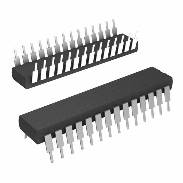
Microchip’s dsPIC33EV family of 16-bit Digital Signal Controllers (DSCs) features a 70 MIPS dsPIC® DSC core with enhanced on-chip features. Capable of operating in harsh environments these devices are suitable for appliance and automotive applications. Rich peripheral integration includes SENT (Single-Edge Nibble Transmission-Transmit/Receive), High Speed PWMs, OP Amps and Error Correcting Code Flash for increased reliability and safety. The performance offered by the dsPIC33EV family of MCUs allows them to be incorporated into the design of high-performance, precision motor control systems that are more energy efficient. They can be used to control BLDC, permanent magnet synchronous, AC induction and stepper motors.
Microcontroller Features 70 MHz Max. CPU Speed
Code-Efficient (C and Assembly) Architecture
16-Bit Wide Data Path
Two 40-Bit Wide Accumulators
Single-Cycle (MAC/MPY) with Dual Data Fetch
Single-Cycle, Mixed-Sign MUL plus Hardware Divide
32-Bit Multiply Support
Intermediate Security for Memory - Provides a Boot Flash Segment in addition to the existing General Flash Segment
Error Code Correction (ECC) for Flash
Added Two Alternate Register Sets for Fast Context Switching
Internal, 15% Low-Power RC (LPRC) – 32 kHz
Internal, 1% Fast RC (FRC) – 7.37 MHz
Internal, 10% Backup RC (BFRC) – 7.37 MHz
Programmable PLLs and Oscillator Clock Sources
Fail-Safe Clock Monitor (FSCM)
Additional Fail-Safe Clock Monitor Source (BFRC), Intended to Provide a Clock Fail Switch Source for the System Clock
Independent Watchdog Timer (WDT)
System Windowed Watchdog Timer (DMT)
Fast Wake-Up and Start-Up
Low-Power Management modes (Sleep, Idle and Doze)
Power Consumption Minimized Executing NOP String
Integrated Power-on Reset (POR) and Brown-out Reset (BOR)
0.5 mA/MHz Dynamic Current (typical)
50 μA at +25°C IPD Current (typical)
Up to Six Pulse-Width Modulation (PWM) Outputs (three generators)
Configurable Analogue to Digital Converter (ADC) Module
Up to 4 Operational Amplifiers
Up to 5 Comparators
Charge Time Measurement Unit (CTMU) - Supports mTouch™ capacitive touch sensing
Five 16-bit Timers
Two 32-bit Timers
Four Output Capture modules Configurable as Timers/Counters
Four Input Capture modules
Two Enhanced Universal Synchronous Asynchronous Receiver Transmitter (EUSART)
Two SPI Modules
One I2C Module with SMBus Support
Feature
- Operating Conditions
- 4.5V to 5.5V, -40ºC to +85ºC, DC to 70 MIPS
- 4.5V to 5.5V, -40ºC to +125ºC, DC to 60 MIPS
- 4.5V to 5.5V, -40ºC to +150ºC, DC to 40 MIPS
- dsPIC33E Core
- Code-Efficient (C and Assembly) Architecture
- Two 40-Bit Wide Accumulators
- Single-Cycle (MAC/MPY) with Dual Data Fetch
- Single-Cycle, Mixed-Sign MUL plus Hardware Divide
- 32-Bit Multiply Support
- Provides a boot Flash segment in addition to the existing general Flash segment
- Error Code Correction (ECC) for Flash
- Added Two Alternate Register Sets for Fast Context Switching
- High-Speed PWM
- Up to Six Pulse-Width Modulation (PWM) Outputs (three generators)
- Primary Master Time Base Inputs allow Time Base Synchronization from Internal/External Sources
- Dead Time for Rising and Falling Edges
- 8.3 ns PWM Resolution at 60 MIPS,
- 16.6 ns Center-Aligned mode at 60 MIPS
- PWM support for DC/DC, AC/DC, inverters, Power Factor Correction (PFC) and lighting
- PWM support for Brushless Direct Current (BLDC), Permanent Magnet Synchronous Motor (PMSM), AC Induction Motor (ACIM), Switched Reluctance Motor (SRM)
- Programmable Fault inputs
- Flexible trigger configurations for Analog-to-Digital conversion
- Independent Time Base
- Supports PWM lock, PWM output chopping and dynamic phase shifting
- Integrated Analog Features
- ADC configurable as 10-bit, 1.1 Msps with four S&H or 12-bit, 500 ksps with one S&H
- Up to 36 analog inputs
- Flexible and Independent ADC Trigger Sources
- Up to Four Op Amp/Comparators with Direct Connection to the ADC module:
- Additional dedicated comparator and 7-bit Digital-to-Analog Converter (DAC)
- Programmable references with 128 voltage points
- Programmable blanking and filtering
- Charge Time Measurement Unit
- Supports mTouch™ capacitive touch sensing
- Provides high-resolution time measurement (1 ns)
- On-chip temperature measurement
- Temperature sensor diode
- Multiple sources of edge input triggers
- Timers/Output Compare/Input Capture
- Up to nine general purpose timers
- Five 16-bit or up to two 32-bit timers/counters, Timer3 can provide ADC trigger
- Four Output Capture modules configurable as timers/counters
- Four Input Capture modules
- Communication Interfaces
- Support for LIN/J2602 bus support and IrDA®
- High and low speed (SCI)
- 25 Mbps data rate without PPS used
- One I2C™ module (up to 1 Mbaud) with SMBus Support
- Two SENT J2716 (Single Edge Nibble Transmission-Transmit/Receive) module for Automotive Applications
- Direct Memory Access (DMA)
- 4-Channel DMA with User-Selectable Priority Arbitration
- Universal Asynchronous Receiver/Transmitter (UART), Serial Peripheral Interface (SPI), ADC, Input Capture, Output Compare
- Qualification and Class B Support
- AEC-Q100 Grade 1 (-40ºC to +125ºC)
- AEC-Q100 Grade 0 (-40ºC to +150ºC)
- Class B Safety Library, IEC 60730
- Functional Safety Features
- Backup FRC
- Windowed WDT uses LPRC
- Windowed Deadman Timer uses System Clock (System Windowed Watchdog Timer)
- H/W Clock Monitor Circuit
- Oscillator Frequency Monitoring through CTMU
- Dedicated PWM Fault Pin
- Lockable Clock Configuration
- Functional Safety support (ISO26262)
- ASIL-B & ASIL-C focused applications
- FMEDA and Safety manual available under NDA upon request to your sales office
- Safety qualified XC16 compiler
- Functional Safety hardware features
- Flash with Error Correction Code (ECC)
- CodeGuard™ Memory Protection
- On-chip Regulator for CPU
- Backup FRC and redundant clock sources
- Fail Safe Clock Monitor
- Windowed Watchdog Timer (WDT)
- Windowed Deadman Timer (DMT)
- Oscillator Frequency Monitoring through CTMU (OSCI, SYSCLK, FRC, BFRC, LPRC)
- BOR and POR
- Analog peripherals redundancies
- Cyclical Redundancy Check (CRC)
- Illegal Opcode Detection
- PWM Lock and Dedicated PWM Fault Pin
- Internal Loopback to test communication peripherals and IO ports
- SFR and Configuration Locks
- Address Trap
- Math Error Trap
- Redundant data storage for Flash-based Configuration bits and Peripheral Pin Select (PPS) Configuration bits

