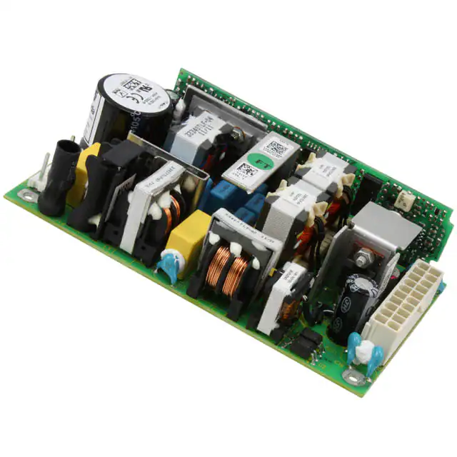
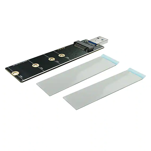
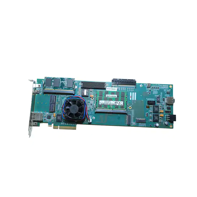
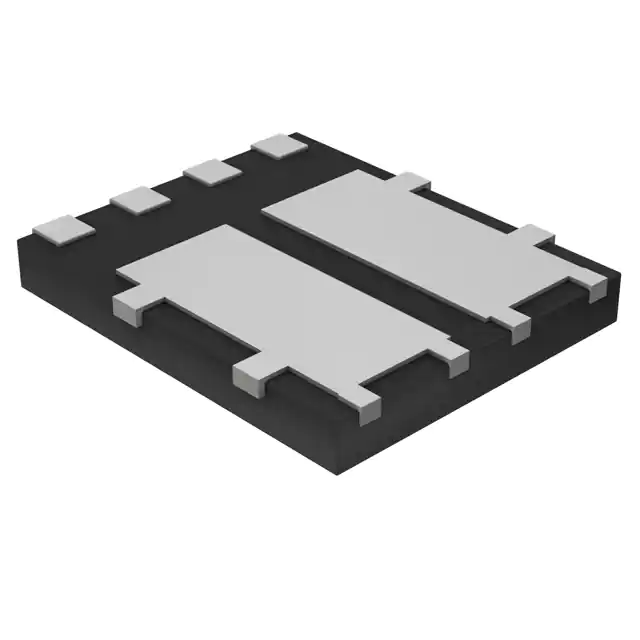
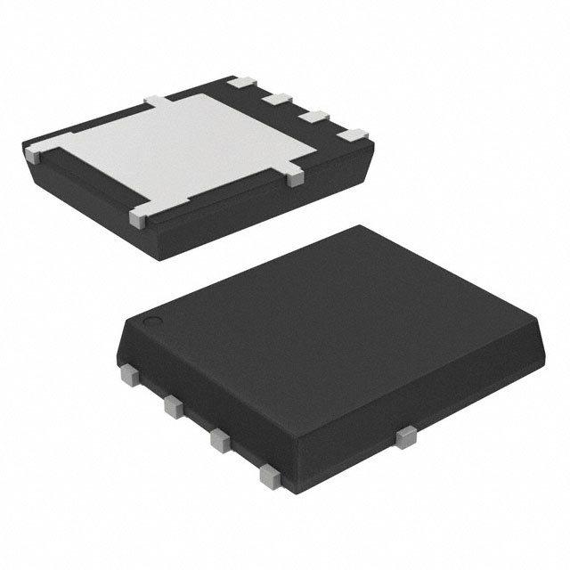
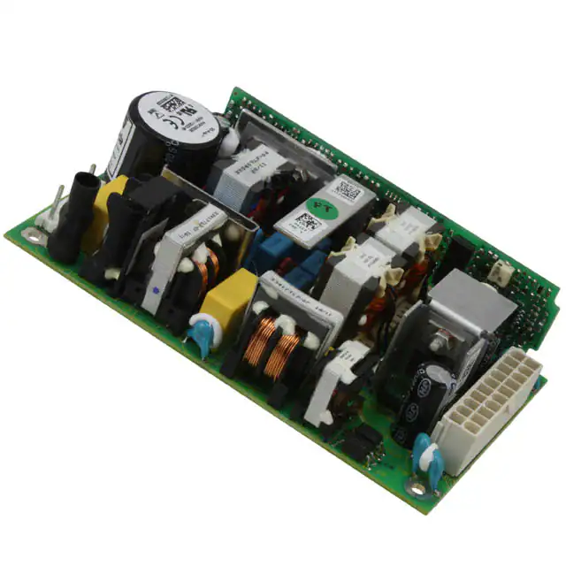
The NVM100015 parts manufactured by TDK-LAMBDA are available for purchase at 9icnet Electronics. Here you can find various types and values of electronic parts from the world's leading manufacturers. The NVM100015 components of 9icnet Electronics are carefully chosen, undergo stringent quality control, and are successfully meet all required standards.
The production status marked on 9icnet.com is for reference only. If you didn't find what you were looking for, you can get more valuable information by emails, such as the NVM100015 Inventory quantity, preferential price, datasheet, and manufacturer. We are always happy to hear from you, so feel free to contact us.
NVLJD4007NZTAG with pin details, that includes NVLJD4007NZ Series, they are designed to operate with a Digi-ReelR Alternate Packaging Packaging, Mounting Style is shown on datasheet note for use in a SMD/SMT, that offers Package Case features such as 6-WDFN Exposed Pad, Technology is designed to work in Si, it has an Operating Temperature range of -55°C ~ 150°C (TJ), the device can also be used as Surface Mount Mounting Type. In addition, the Number of Channels is 2 Channel, the device is offered in 6-WDFN (2x2) Supplier Device Package, the device has a Dual of Configuration, and FET Type is 2 N-Channel (Dual), and the Power Max is 755mW, and Transistor Type is 2 N-Channel, and the Drain to Source Voltage Vdss is 30V, and Input Capacitance Ciss Vds is 20pF @ 5V, and the FET Feature is Logic Level Gate, and Current Continuous Drain Id 25°C is 245mA, and the Rds On Max Id Vgs is 7 Ohm @ 125mA, 4.5V, and Vgs th Max Id is 1.5V @ 100μA, and the Gate Charge Qg Vgs is 0.75nC @ 4.5V, and Pd Power Dissipation is 755 mW, it has an Maximum Operating Temperature range of + 150 C, it has an Minimum Operating Temperature range of - 55 C, and the Fall Time is 72 ns, and Rise Time is 41 ns, and the Vgs Gate Source Voltage is 10 V, and Id Continuous Drain Current is 245 mA, and the Vds Drain Source Breakdown Voltage is 30 V, and Rds On Drain Source Resistance is 1.4 Ohms, and the Transistor Polarity is N-Channel, and Typical Turn Off Delay Time is 96 ns, and the Typical Turn On Delay Time is 9 ns, and Qg Gate Charge is 0.75 nC.
NVLJD4007NZTBG with user guide, that includes 1.5V @ 100μA Vgs th Max Id, they are designed to operate with a 30 V Vds Drain Source Breakdown Voltage, Transistor Type is shown on datasheet note for use in a 2 N-Channel, that offers Transistor Polarity features such as N-Channel, Technology is designed to work in Si, as well as the 6-WDFN (2x2) Supplier Device Package, the device can also be used as NVLJD4007NZ Series. In addition, the Rds On Max Id Vgs is 7 Ohm @ 125mA, 4.5V, the device is offered in 7 Ohms Rds On Drain Source Resistance, the device has a 755mW of Power Max, and Packaging is Tape & Reel (TR), and the Package Case is 6-WDFN Exposed Pad, it has an Operating Temperature range of -55°C ~ 150°C (TJ), and the Number of Channels is 2 Channel, and Mounting Style is SMD/SMT, and the Mounting Type is Surface Mount, and Input Capacitance Ciss Vds is 20pF @ 5V, and the Id Continuous Drain Current is 245 mA, and Gate Charge Qg Vgs is 0.75nC @ 4.5V, and the FET Type is 2 N-Channel (Dual), and FET Feature is Logic Level Gate, and the Drain to Source Voltage Vdss is 30V, and Current Continuous Drain Id 25°C is 245mA.
NVLUS4C12NTAG with circuit diagram manufactured by ON Semiconductor. is part of the ESD Suppressors, , and with support for ESD Suppressors COMP UDFN6 30V 10.7A, N-Channel 30V 6.8A (Ta) 630mW (Ta) Surface Mount 6-UDFN (2x2), Trans MOSFET N-CH 30V 10.7A Automotive 6-Pin UDFN EP T/R.

