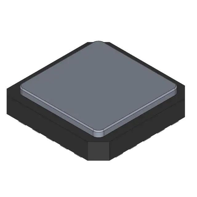
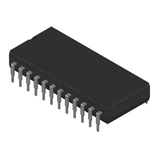
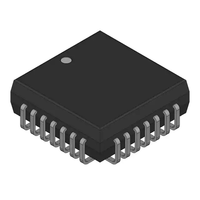
The ’HC174 and ’HCT174 are edge triggered flip-flops which utilize silicon gate CMOS circuitry to implement D-type flip-flops. They possess low power and speeds comparable to low power Schottky TTL circuits. The devices contain six master-slave flip-flops with a common clock and common reset. Data on the D input having the specified setup and hold times is transferred to the Q output on the low to high transition of the CLOCK input. The MR\ input, when low, sets all outputs to a low state.
Each output can drive ten low power Schottky TTL equivalent loads. The ’HCT174 is functional as well as, pin compatible to the ’LS174.
Feature
- Buffered Positive Edge Triggered Clock
- Asynchronous Common Reset
- Fanout (Over Temperature Range)
- Standard Outputs. . . . . . . . . . . . . . . 10 LSTTL Loads
- Bus Driver Outputs . . . . . . . . . . . . . 15 LSTTL Loads
- Wide Operating Temperature Range . . . -55°C to 125°C
- Balanced Propagation Delay and Transition Times
- Significant Power Reduction Compared to LSTTL Logic ICs
- HC Types
- 2V to 6V Operation
- High Noise Immunity: NIL = 30%, NIH = 30% of VCC at VCC = 5V
- HCT Types
- 4.5V to 5.5V Operation
- Direct LSTTL Input Logic Compatibility, VIL = 0.8V (Max), VIH = 2V (Min)
- CMOS Input Compatibility, Il1μA at VOL, VOH
The ’HC174 and ’HCT174 are edge triggered flip-flops which utilize silicon gate CMOS circuitry to implement D-type flip-flops. They possess low power and speeds comparable to low power Schottky TTL circuits. The devices contain six master-slave flip-flops with a common clock and common reset. Data on the D input having the specified setup and hold times is transferred to the Q output on the low to high transition of the CLOCK input. The MR\ input, when low, sets all outputs to a low state.
Each output can drive ten low power Schottky TTL equivalent loads. The ’HCT174 is functional as well as, pin compatible to the ’LS174.


