
Widebus is a trademark of Texas Instruments. (1) Component qualification in accordance with JEDEC and industry standards to ensure reliable operation over an extended temperature range. This includes, but is not limited to, Highly Accelerated Stress Test (HAST) or biased 85/85, temperature cycle, autoclave or unbiased HAST, electromigration, bond intermetallic life, and mold compound life. Such qualification testing should not be viewed as justifying use of this component beyond specified performance and environmental limits.
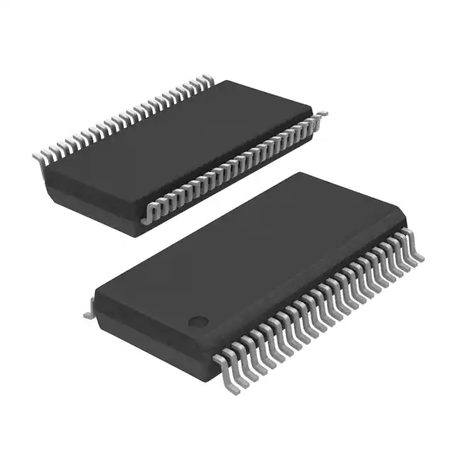
DescriptionThe SN74LVTH162373 is a16-bit transparent D-type latch with 3-state outputs designed for low-voltage (3.3-V) VCC operation, but with the capability to provide a TTL interface to a 5-V system environment. This device is particularly suitable for implementing buffer registers, I/O ports, bidirectional bus drivers, and working registers.
A buffered output-enable ( series resistors to reduce overshoot and undershoot.
Active bus-hold circuitry holds unused or undriven inputs at a valid logic state. Use of pullup or pulldown resistors with the bus-hold circuitry is not recommended.
When VCC is between 0 and 1.5 V, the device is in the high-impedance state during power up or power down. However, to ensure the high-impedance state above 1.5 V, OE should be tied to VCC through a pullup resistor; the minimum value of the resistor is determined by the current-sinking capability of the driver.
This device is fully specified for hot-insertion applications using Ioff and power-up 3-state. The Ioff circuitry disables the outputs, preventing damaging current backflow through the device when it is powered down. The power-up 3-state circuitry places the outputs in the high-impedance state during power up and power down, which prevents driver conflict.
This device can be used as two 8-bit latches or one 16-bit latch. When the latch-enable (LE) input is high, the Q outputs follow the data (D) inputs. When LE is taken low, the Q outputs are latched at the levels set up at the D inputs.
Feature
- Controlled Baseline
- One Assembly/Test Site, One Fabrication Site
- Extended Temperature Performance of -55°C to 125°C
- Enhanced Diminishing Manufacturing Sources (DMS) Support
- Enhanced Product-Change Notification
- Qualification Pedigree(1)
- Member of the Texas Instruments Widebus? Family
- Output Ports Have Equivalent 22- Series Resistors, So No External Resistors Are Required
- Supports Mixed-Mode Signal Operation (5-V Input and Output Voltages With 3.3-V VCC)
- Supports Unregulated Battery Operation Down to 2.7 V
- Typical VOLP (Output Ground Bounce) <:0.8 V at VCC = 3.3 V, TA = 25°C
- Ioff and Power-Up 3-State Support Hot Insertion
- Bus Hold on Data Inputs Eliminates the Need for External Pullup/Pulldown Resistors
- Distributed VCC and GND Pins Minimize High-Speed Switching Noise
- Flow-Through Architecture Optimizes PCB Layout
- Latch-Up Performance Exceeds 500 mA Per JESD 17
- ESD Protection Exceeds JESD 22
- 2000-V Human-Body Model (A114-A)
- 200-V Machine Model (A115-A)
Widebus is a trademark of Texas Instruments. (1) Component qualification in accordance with JEDEC and industry standards to ensure reliable operation over an extended temperature range. This includes, but is not limited to, Highly Accelerated Stress Test (HAST) or biased 85/85, temperature cycle, autoclave or unbiased HAST, electromigration, bond intermetallic life, and mold compound life. Such qualification testing should not be viewed as justifying use of this component beyond specified performance and environmental limits.
DescriptionThe SN74LVTH162373 is a16-bit transparent D-type latch with 3-state outputs designed for low-voltage (3.3-V) VCC operation, but with the capability to provide a TTL interface to a 5-V system environment. This device is particularly suitable for implementing buffer registers, I/O ports, bidirectional bus drivers, and working registers.
A buffered output-enable ( series resistors to reduce overshoot and undershoot.
Active bus-hold circuitry holds unused or undriven inputs at a valid logic state. Use of pullup or pulldown resistors with the bus-hold circuitry is not recommended.
When VCC is between 0 and 1.5 V, the device is in the high-impedance state during power up or power down. However, to ensure the high-impedance state above 1.5 V, OE should be tied to VCC through a pullup resistor; the minimum value of the resistor is determined by the current-sinking capability of the driver.
This device is fully specified for hot-insertion applications using Ioff and power-up 3-state. The Ioff circuitry disables the outputs, preventing damaging current backflow through the device when it is powered down. The power-up 3-state circuitry places the outputs in the high-impedance state during power up and power down, which prevents driver conflict.
This device can be used as two 8-bit latches or one 16-bit latch. When the latch-enable (LE) input is high, the Q outputs follow the data (D) inputs. When LE is taken low, the Q outputs are latched at the levels set up at the D inputs.


