Description
Intel’s 28F020 CMOS flash memory offers the most cost-effective and reliable alternative for read/write random access nonvolatile memory. The 28F020 adds electrical chip-erasure and reprogramming to familiar EPROM technology. Memory contents can be rewritten: in a test socket; in a PROM-programmer socket; onboard during subassembly test; in-system during final test; and in-system after sale. The 28F020 increases memory flexibility, while contributing to time and cost savings.
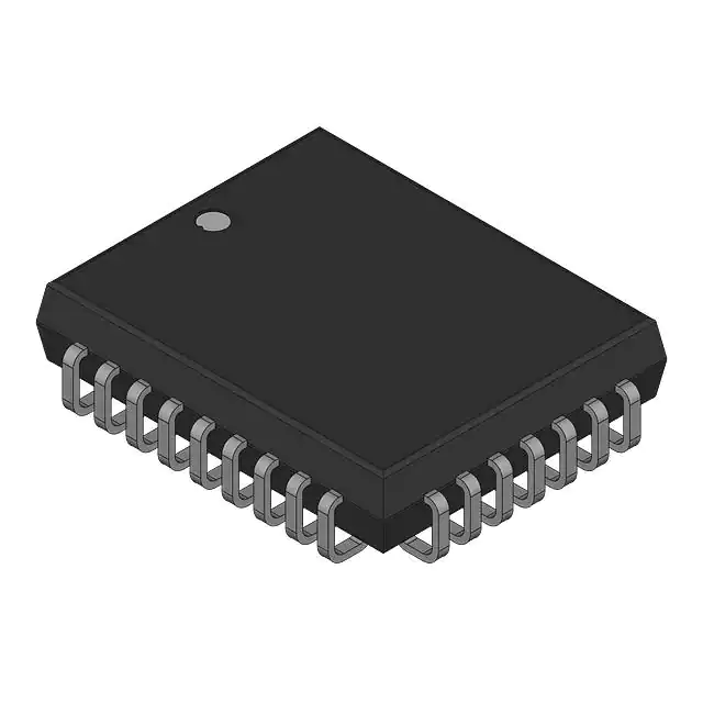
The 28F020 is a 2048-kilobit nonvolatile memory organized as 262,144 bytes of eight bits. Intel’s 28F020 is offered in 32-pin plastic DIP, 32-lead PLCC, and 32-lead TSOP packages. Pin assignments conform to JEDEC standards for byte-wide EPROMs.
Extended erase and program cycling capability is designed into Intel’s ETOX™ (EPROM Tunnel Oxide) process technology. Advanced oxide processing, an optimized tunneling structure, and lower electric field combine to extend reliable cycling beyond that of traditional EEPROMs. With the 12.0 V VPP supply, the 28F020 performs 100,000 erase and program cycles—well within the time limits of the quick-pulse programming and quick-erase algorithms.
Intel’s 28F020 employs advanced CMOS circuitry for systems requiring high-performance access speeds, low power consumption, and immunity to noise. Its 90 ns access time provides zero wait-state performance for a wide range of microprocessors and microcontrollers. Maximum standby current of 100 µA translates into power savings when the device is deselected. Finally, the highest degree of latch-up protection is achieved through Intel’s unique EPI processing. Prevention of latch-up is provided for stresses up to 100 mA on address and data pins, from –1 V to VCC + 1 V.
With Intel’s ETOX process technology base, the 28F020 builds on years of EPROM experience to yield the highest levels of quality, reliability, and cost-effectiveness.
Features
■Flash Electrical Chip-Erase
-2Second Typical Chip-Erase
■Quick-Pulse Programming Algorithm
-10μS Typical Byte-Program
-4second Chip-Program
■100,000 Erase/Program Cycles
■12.0V±5%VPP
■High-Performance Read
-90ns Maximum Access Time
■CMOS Low Power Consumption
-10mA Typical Active Current
-50 μA Typical Standby Current
-0Watts Data Retention Power
■Integrated Program/Erase Stop Timer
■ Command Register Architecture for Microprocessor/Microcontroller Compatible Write Interface
■ Noise Immunity Features
-±10%Vcc Tolerance
-Maximum Latch-Up lmmunity through EPI Processing
■ ETOXTM Nonvolatile Flash Technology
-EPROM-Compatible Process Base
-High-Volume Manufacturing Experience
■ JEDEC-Standard Pinouts
-32-Pin Plastic Dip
-32-Lead PLCC
-32-Lead TSOP
(See Packaging Spec,Order #231369)
■ Extended Temperature Options
(Picture: Pinout)


