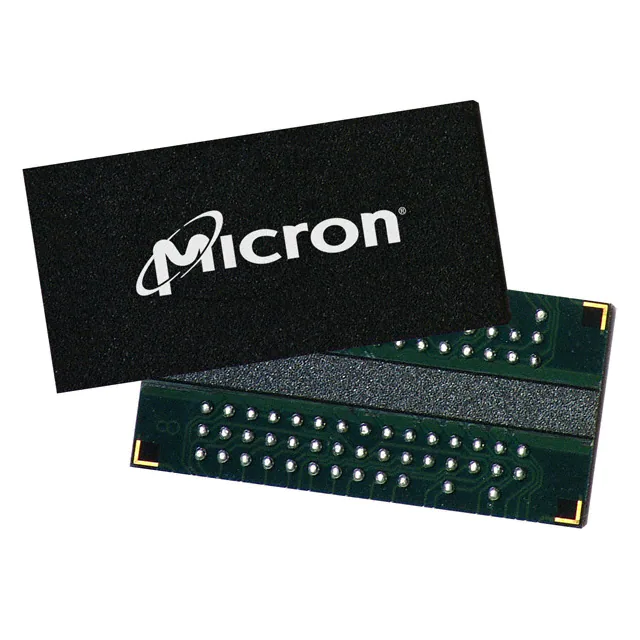
The DDR2 SDRAM uses a double data rate architecture to achieve high-speed operation. The double data rate architecture is essentially a 4n-prefetch architecture, with an interface designed to transfer two data words per clock cycle at the I/O balls. A single read or write access for the DDR2 SDRAM effectively consists of a single 4n-bit-wide, one-clock-cycle data transfer at the internal DRAM core and four corresponding n-bitwide, one-half-clock-cycle data transfers at the I/O balls. A bidirectional data strobe (DQS, DQS#) is transmitted externally, along with data, for use in data capture at the receiver. DQS is a strobe transmitted by the DDR2 SDRAM during READs and by the memory controller during WRITEs. DQS is edge-aligned with data for READs and center-aligned with data for WRITEs. The x16 offering has two data strobes, one for the lower byte (LDQS, LDQS#) and one for the upper byte (UDQS, UDQS#).
Feature
• VDD = 1.8V ±0.1V, VDDQ = 1.8V ±0.1V
• JEDEC-standard 1.8V I/O (SSTL_18-compatible)
• Differential data strobe (DQS, DQS#) option
• 4n-bit prefetch architecture
• Duplicate output strobe (RDQS) option for x8
• DLL to align DQ and DQS transitions with CK
• 4 internal banks for concurrent operation
• Programmable CAS latency (CL)
• Posted CAS additive latency (AL)
• WRITE latency = READ latency - 1 t CK
• Selectable burst lengths (BL): 4 or 8
• Adjustable data-output drive strength
• 64ms, 8192-cycle refresh
• On-die termination (ODT)
• Industrial temperature (IT) option
• Automotive temperature (AT) option
• RoHS-compliant
• Supports JEDEC clock jitter specification
(Picture:Pinout / Diagram)


