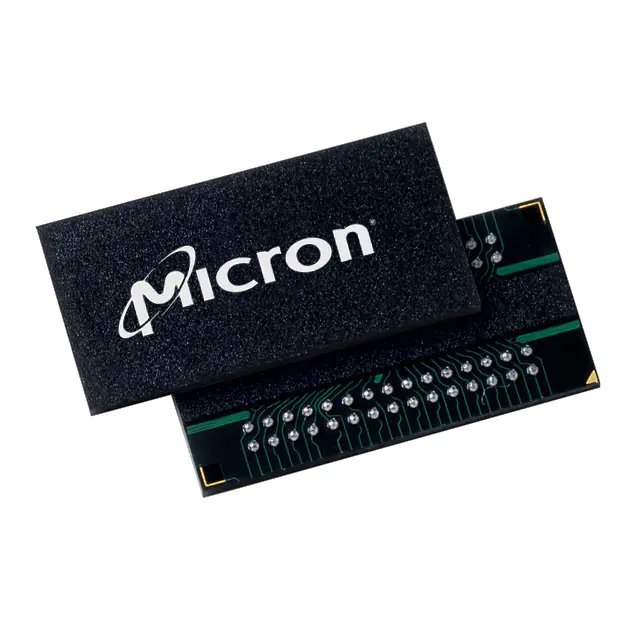
The DDR SDRAM's MT46V32M8BG-5B:GTR uses a double data rate architecture to achieve high-speed operation. The double data rate architecture is essentially a 2n-prefetch architecture with an interface designed to transfer two data words per clock cycle at the I/O pins. A single read or write access for The MT46V32M8BG-5B:GTR effectively consists of a single 2n-bit-wide, one-clockcycle data transfer at the internal DRAM core and two corresponding n-bit-wide, onehalf-clock-cycle data transfers at the I/O pins. A bidirectional data strobe (DQS) is transmitted externally, along with data, for use in data capture at the receiver. DQS is a strobe transmitted by The MT46V32M8BG-5B:GTR during READs and by the memory controller during WRITEs. DQS is edge-aligned with data for READs and center-aligned with data for WRITEs. The x16 offering has two data strobes, one for the lower byte and one for the upper byte.
The MT46V32M8BG-5B:GTR operates from a differential clock (CK and CK#); the crossing of CK going HIGH and CK# going LOW will be referred to as the positive edge of CK. Commands (address and control signals) are registered at every positive edge of CK. Input data is registered on both edges of DQS, and output data is referenced to both edges of DQS, as well as to both edges of CK. Read and write accesses to The MT46V32M8BG-5B:GTR are burst oriented; accesses start at a selected location and continue for a programmed number of locations in a programmed sequence. Accesses begin with the registration of an ACTIVE command, which may then be followed by a READ or WRITE command. The address bits registered coincident with the ACTIVE command are used to select the bank and row to be accessed. The address bits registered coincident with the READ or WRITE command are used to select the bank and the starting column location for the burst access.
The MT46V32M8BG-5B:GTR provides for programmable READ or WRITE burst lengths of 2, 4, or 8 locations. An auto precharge function may be enabled to provide a self-timed row precharge that is initiated at the end of the burst access.
Feature
• VDD = +2.5V ±0.2V, VDDQ = +2.5V ±0.2V
• VDD = +2.6V ±0.1V, VDDQ = +2.6V ±0.1V (DDR400)
• Bidirectional data strobe (DQS) transmitted/ received with data, that is, source-synchronous data capture (x16 has two – one per byte)
• Internal, pipelined double-data-rate (DDR) architecture; two data accesses per clock cycle
• Differential clock inputs (CK and CK#)
• Commands entered on each positive CK edge
• DQS edge-aligned with data for READs; centeraligned with data for WRITEs
• DLL to align DQ and DQS transitions with CK
• Four internal banks for concurrent operation
• Data mask (DM) for masking write data (x16 has two – one per byte)
• Programmable burst lengths (BL): 2, 4, or 8
• Auto refresh
– 64ms, 8192-cycle(Commercial & Industrial)
– 16ms, 8192-cycle (Automotive)
• Self refresh (not available on AT devices)
• Longer-lead TSOP for improved reliability (OCPL)
• 2.5V I/O (SSTL_2-compatible)
• Concurrent auto precharge option supported
• tRAS lockout supported (t RAP = t RCD)


