Functional Description
P5Q serial phase change memory (PCM) is nonvolatile memory that stores information through a reversible structural phase change in a chalcogenide material. The material exhibits a change in material properties, both electrical and optical, when changed from the amorphous (disordered) to the polycrystalline (regularly ordered) state. In the case of PCM, information is stored via the change in resistance that the chalcogenide material experiences when undergoing a phase change. The material also changes optical properties after experiencing a phase change, a characteristic that has been successfully mastered for use in current rewritable optical storage devices, such as rewritable CDs and DVDs. The P5Q serial PCM storage element consists of a thin film of chalcogenide contacted by a resistive heating element. In PCM, the phase change is induced in the memory cell by highly localized Joule heating caused by an induced current at the material junction. During a WRITE operation, a small volume of the chalcogenide material is made to change phase. The phase change is a reversible process and is modulated by the magnitude of injected current, the applied voltage, and the duration of the heating pulse. Unlike other proposed alternative memories, P5Q serial PCM technology uses a conventional CMOS process with the addition of a few additional layers to form the memory storage element. Overall, the basic memory manufacturing process used to make PCM is less complex than that of NAND, NOR, or DRAM. P5Q serial PCM combines the benefits of traditional floating gate Flash, both NOR-type and NAND-type, with some of the key attributes of RAM and EEPROM. Like NOR Flash and RAM technology, PCM offers fast random access times. Like NAND Flash, PCM has the ability to write moderately fast, and like RAM and EEPROM, PCM supports bit-alterable WRITEs (overwrite). Unlike Flash, no separate erase step is required to change information from 0 to 1 and 1 to 0. Unlike RAM, however, the technology is nonvolatile with data retention compared with NOR Flash.
Features
• SPI bus compatible serial interface
• Maximum clock frequency
– 66 MHz (0°C to +70°C)
– 33 MHz (–30°C to +85°C)
• 2.7V to 3.6V single supply voltage
• Supports legacy SPI protocol and new quad I/O or dual I/O SPI protocol
• Quad I/O frequency of 50 MHz, resulting in an equivalent clock frequency up to 200 MHz
• Dual I/O frequency of 66 MHz, resulting in an equivalent clock frequency up to 132 MHz
• Continuous READ of entire memory via single
instruction:
– Quad and dual output fast read
– Quad and dual input fast program
• Uniform 128Kb sectors (Flash emulation)
• WRITE operations
– 128Kb sectors ERASE (emulated)
– Legacy Flash PAGE PROGRAM
– Bit-alterable page WRITEs
– PAGE PROGRAM on all 1s (PRESET WRITEs)
• Write protections: protected area size defined by four nonvolatile bits (BP0, BP1, BP2, and BP3)
• JEDEC-standard two-byte signature (DA18h)
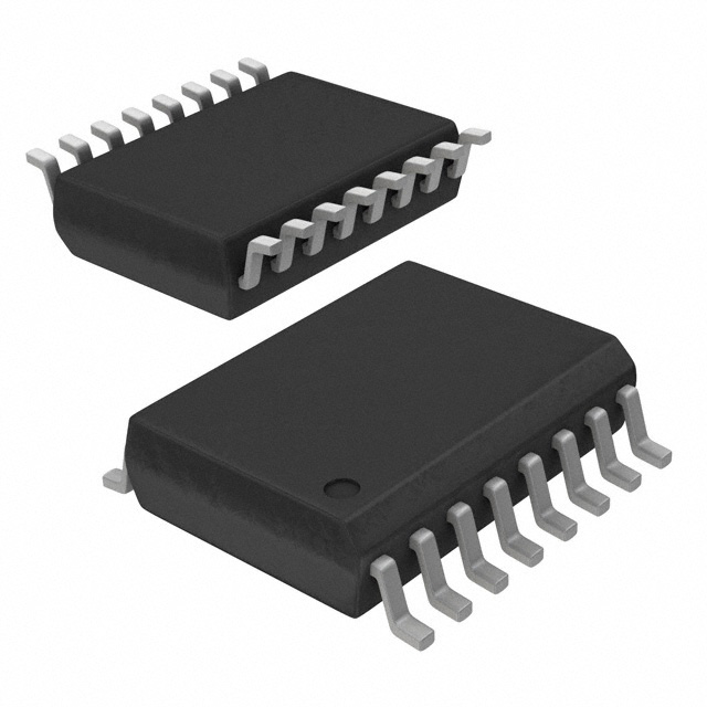
• 128Mb density with SOIC16 package
• More than 1,000,000 WRITE cycles
• Phase change memory (PCM)
– Chalcogenide phase change storage element
– Bit-alterable WRITE operation
(Picture: Pinout)


