
The M29W is an asynchronous, uniform block, parallel NOR Flash memory device manufactured on 90nm single-level cell (SLC) technology. READ, ERASE, and PROGRAM operations are performed using a single low-voltage supply. Upon power-up, the device defaults to read array mode. 128Mb 3V Embedded Parallel NOR Flash.
The main memory array is divided into uniform blocks that can be erased independently so that valid data can be preserved while old data is purged. PROGRAM and ERASE commands are written to the command interface of the memory. An on-chip program/ erase controller simplifies the process of programming or erasing the memory by taking care of all special operations required to update the memory contents. The end of a PROGRAM or ERASE operation can be detected and any error condition can be identified. The command set required to control the device is consistent with JEDEC standards.
CE#, OE#, and WE# control the bus operation of the device and enable a simple connection to most microprocessors, often without additional logic. The M29W supports asynchronous random read and page read from all blocks of the array. It features a write to buffer program capability that improves throughput by programming a buffer of 32 words in one command sequence. Also, in x16 mode, the enhanced buffered program capability improves throughput by programming 256 words in one command sequence. The device VPP/WP# signal enables faster programming.
The device contains a 128-word (x16) and 256-byte (x8) extended memory block. The user can program this additional space and then protect it to permanently secure the contents. The device also features different levels of hardware and software protection to secure blocks from unwanted modification.
Features
• Supply voltage
– VCC = 2.7–3.6V (program, erase, read)
– VCCQ = 1.65–3.6V (I/O buffers)
– VPPH = 12V for fast program (optional)
• Asynchronous random/page read
– Page size: 8 words or 16 bytes
– Page access: 25, 30ns
– Random access: 60ns1, 70, 80ns
• Fast program commands: 32-word (64-byte) write buffer
• Enhanced buffered program commands: 256-word
• Program time
– 16µs per byte/word TYP
– Chip program time: 5s with VPPH and 8s without VPPH
• Memory organization
– Uniform blocks: 128 main blocks, 128-Kbytes or 64-Kwords each
• Program/erase controller
– Embedded byte/word program algorithms
• Program/erase suspend and resume capability
– Read from any block during a PROGRAM SUSPEND operation
– Read or program another block during an ERASE SUSPEND operation
• Unlock bypass, block erase, chip erase, write to buffer, enhanced buffer program commands
– Fast buffered/batch programming
– Fast block/chip erase
• VPP/WP# pin protection
– Protects first or last block regardless of block protection settings
• Software protection
– Volatile protection
– Nonvolatile protection
– Password protection
• Extended memory block
– 128-word (256-byte) memory block for permanent, secure identification
• Common flash interface
– 64-bit security code
• Low power consumption: Standby and automatic mode
• Minimum 100,00 PROGRAM/ERASE cycles per block
• RoHS compliant packages
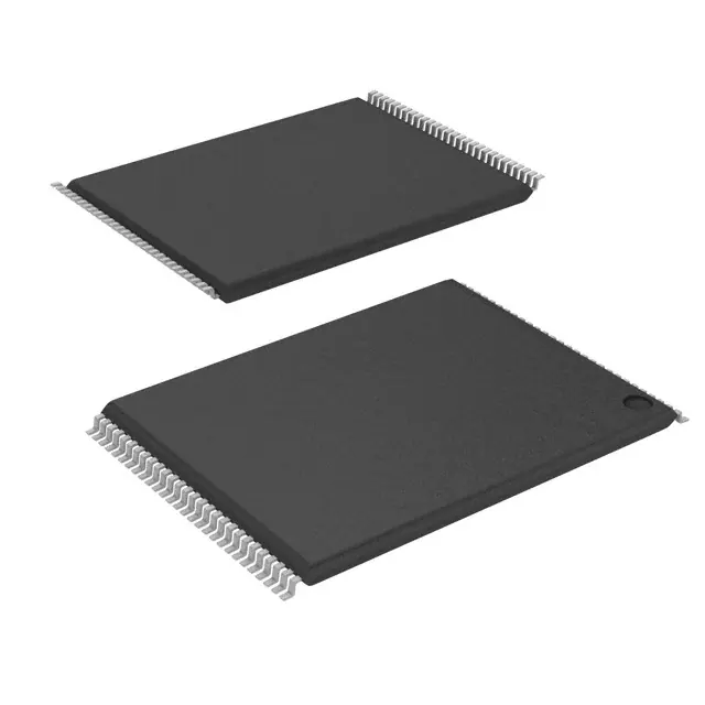
– 56-pin TSOP (N) 14mm x 20mm
– 64-ball TBGA (ZA) 10mm x 13mm
– 64-ball FBGA (ZS) 11mm x 13mm
• Electronic signature
– Manufacturer code: 0020h
– M29W128GH uniform, last block protected by VPP/WP#: 227Eh + 2221h + 2201h
– M29W128GL uniform, first block protected by VPP/WP#: 227Eh + 2221h + 2200h
• Automotive device grade temperature
– –40°C to +125°C (automotive grade certified)


