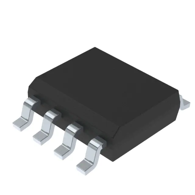
Fully supports Quick Charge 2.0 specification Class 9 V, and 12 V output voltage Class 12 V, and 20 V output voltage USB battery charging specification revision 1.2 compatible Automatic USB DCP shorting to D- line Default 5 V mode operation Supports TOPSwitch and TinySwitch Very low power consumption Below 5 V output Fail safe operation Adjacent pin-to-pin short-circuit fault Open circuit pin fault
Typical Applications Battery chargers for smart phones, tablets, netbooks, digital cameras, and bluetooth accessories USB power output ports
Descriptionis a low-cost USB high-voltage dedicated charging port (HVDCP) interface IC for the Quick Charge 2.0 specification. It incorporates all necessary functions to add Quick Charge 2.0 capability to Power Integrations' switcher ICs such as TOPSwitch or TinySwitch and other solutions employing traditional feedback schemes.
CHY100 supports the full output voltage range of either Class A or Class B. Optionally Class B can be inhibited for protecting the battery charger from accidental damage. CHY100 automatically detects whether a connected Powered Device (PD) is Quick Charge 2.0 capable before enabling output voltage adjustment. a PD not compliant to Quick Charge 2.0 is detected the CHY100 disables output voltage adjustment to ensure safe operation with legacy 5 V only USB PDs.
GROUND (GND) Pin Ground. V1 Pin Open Drain input of output voltage adjustment switch. Active for 12 V, and 20 V output setting. V2 Pin Open Drain input of output voltage adjustment switch. Active for 12 V, and 20 V output setting. V3 Pin Open Drain input of output voltage adjustment switch. Active for 20 V output setting. BYPASS (BP) Pin Connection point for an external bypass capacitor for the internally generated supply voltage. REFERENCE (R) Pin Connected to internal band-gap reference. Provides reference current through connected resistor. DATA LINE D+ Pin USB D+ data line input. DATA LINE D- Pin USB D- data line input.
is a low-cost USB high-voltage dedicated charging port (HVDCP) interface IC for the Quick Charge 2.0 specification. It incorporates all necessary functions to add Quick Charge 2.0 capability to Power Integrations' integrated switcher ICs such as TOPSwitch or TinySwitch. CHY100 also supports other solutions with traditional feedback schemes like optocoupler and secondary reference regulator TL431 as depicted in Figure 5.
Reference Input Resister RREF at the REFERENCE pin is connected to an internal band gap reference and provides an accurate reference current for internal timing circuits. The recommended value is RREF 127 k. Quick Charge 2.0 Interface At power-up CHY100 turns on switch N5 (see Figure ms or less after the BYPASS pin voltage has reached 4 V. Switch N4 and output switches to N3 remain off. This sets the default 5 V output voltage level. With D+ and D- short-circuited the normal handshake between the AC-DC adapter (DCP) and powered devices (PD) as described in the USB Battery Charging Specification 1.2 can commence. After switch N5 has been turned on CHY100 starts monitoring the voltage level at D+. If it continuously stays above 0.325 V for at least 1.25 seconds CHY100 will enter Quick Charge 2.0 operation mode. If the voltage at D+ drops any time below V CHY100 resets the 1.25 seconds timer and stays in USB Battery Charging Specification 1.2 compatibility mode with a default output voltage 5 V. Once CHY100 has entered Quick Charge 2.0 operation mode switch N5 will be turned off. Additionally switch N4 is turned on connecting 19.53 k pull-down resistor to D-. As soon as the voltage at D- has dropped low (<0.325 V) for at least ms CHY100 starts accepting requests for different AC-DC adapter output voltages by means of applied voltage levels at data lines D+ and D- through the powered device. Table 1 summarizes the output voltage lookup table, corresponding AC-DC adapter output voltages and status of switches 0.6 V
CHY100 supports the full output voltage range of Quick Charge 2.0 Class V) or Class or 20 V). It automatically detects either Quick Charge 2.0 capable powered devices (PD) or legacy PDs compliant with the USB Battery Charging Specification revision 1.2 and only enables output voltage adjustment accordingly. Shunt Regulator The internal shunt regulator clamps the BYPASS pin 6 V when current is provided through an external resistor (RBP in Figure 5). This facilitates powering of CHY100 externally over the wide power supply output voltage range 20 V. Recommended values are RBP 4.53 k and CBP = 220 nF. BYPASS Pin Undervoltage The BYPASS pin undervoltage circuitry resets the CHY100 when the BYPASS pin voltage drops below 3.9 V. Once the BYPASS pin voltage drops below V it must rise back V to enable correct operation.
Requests made by a connected powered device to set 12 V output voltage can be inhibited by connecting the V2 pin to the BYPASS pin (either directly or through a resistor 100 k This will also inhibit requests for 20 V output. Connecting the V3 pin to BYPASS (directly or through a resistor k ) will inhibit any requests for setting 20 V output. At USB cable disconnect the voltage level D+ is pulled down by resistor RDAT(LKG) (see Figure 5). Once it drops below V CHY100 will turn on switch N5 (thereby short-circuiting D+ and D-) and turns off switches to N4. This sets the default output voltage 5 V. The recommended value for RDAT(LKG) 390 k.


