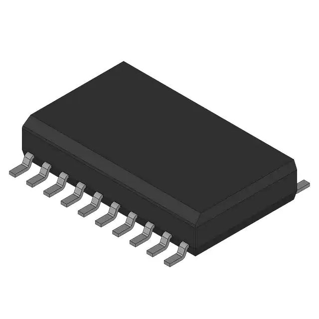
The TDA3681ATH/N1S,518 is a multiple output voltage regulator with a power switch and an ignition buffer. It is intended for use in car radios with or without a microcontroller. The TDA3681ATH/N1S,518 contains the following:
- Four fixed voltage regulators with a foldback current protection (regulators 1, 2, 3 and 4). Regulator 2, which is intended to supply a microcontroller, also operates during load dump and thermal shutdown
- Regulators 3 and 4 have a second supply pin that can be connected to a lower supply voltage (>6.5 V) to reduce the power dissipation
- A power switch with protection, operated by a control input
- Reset and hold outputs that can be used to interface with the microcontroller; the reset signal can be used to call up the microcontroller
- Both supply pins can withstand load dump pulses and negative supply voltages
- Regulator 2, which is in regulation at a backup voltage above 6.5 V
- A provision for the use of a reserve supply capacitor that will hold enough energy for regulator 2 (5 V continuous) to allow a microcontroller to prepare for loss of voltage
- An ignition input Schmitt trigger with push-pull output stage.
Feature
- Low noise behaviour and good stability with very small output capacitors
- Second supply pin for regulators 3 and 4 to reduce power dissipation (e.g. via a DC-to-DC converter)
- Three VP -state controlled regulators (regulators 1, 3 and 4) and a power switch
- Regulator 2, reset and ignition buffer operational during load dump and thermal shutdown
- Combined control pin for switching regulators 1 and 3
- Separate control pins for switching regulator 4 and the power switch
- Supply voltage range from -18 to +50 V
- Low quiescent current in standby mode (when regulators 1, 3 and 4 and power switch are switched off and ignition input is low)
- Hold output (open-collector output stage) for low VP (regulators 1, 3 and 4 and power switch off)
- Hold output when one of regulators 1 and 3 and/or 4 is out of regulation
- Hold output for foldback mode of power switch and regulators 1, 3 and 4
- Hold output for load dump and temperature protection
- Reset (push-pull output stage) for regulator 2
- Adjustable reset delay time
- High supply voltage ripple rejection
- Backup capacitor for regulator 2
- One independent ignition buffer (active HIGH).
- Reverse polarity safe (down to -18 V without high reverse current)
- Able to withstand voltages up to 18 V at the outputs (supply line may be short-circuited)
- ESD protection on all pins
- Thermal protections
- Load dump protection
- Foldback current limit protection for regulators 1, 2, 3 and 4
- Delayed second current limit protection for the power switch (at short-circuit)
- The regulator outputs and the power switch are DC short-circuit safe to ground and supply (VP ).


