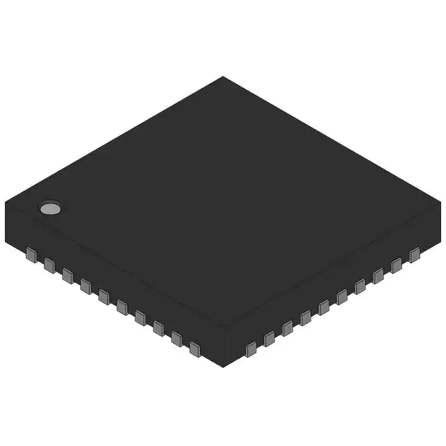
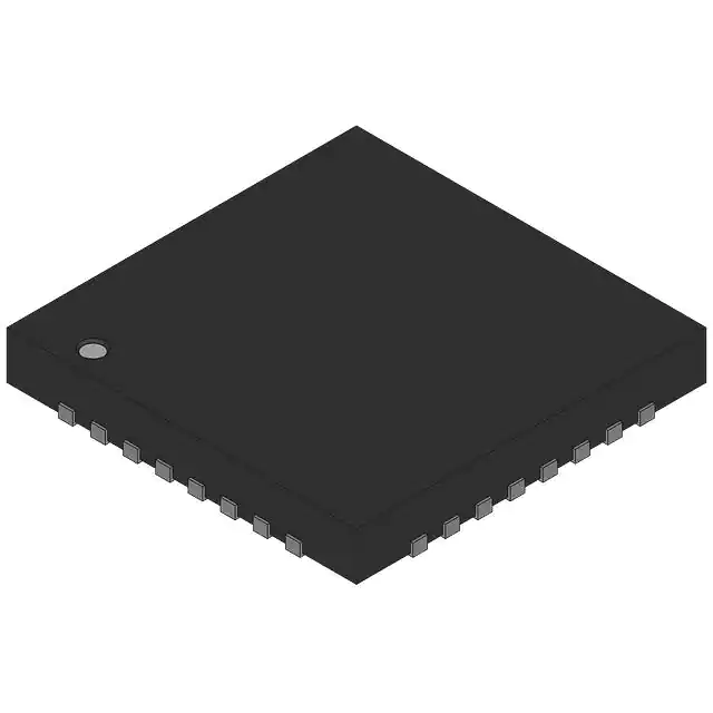
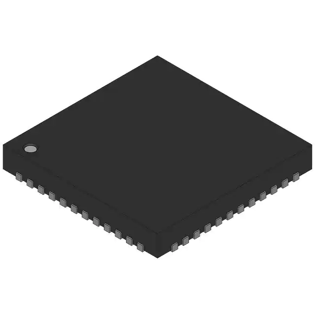
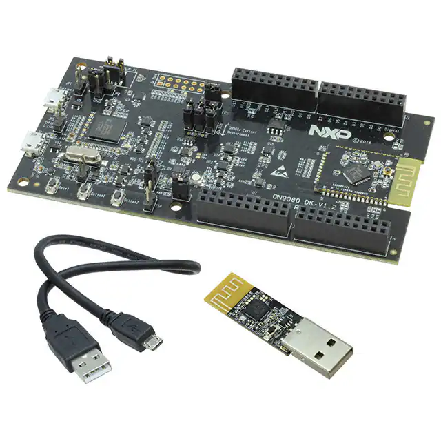
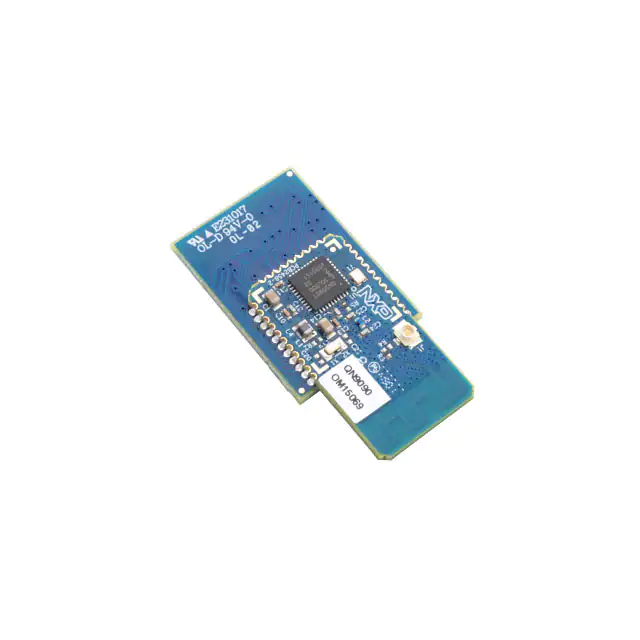
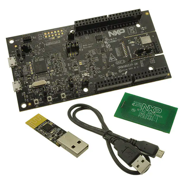
QN9080CHNY is an ultra-low-power, high-performance and highly integrated Bluetooth Low Energy solution for Bluetooth® Smart applications such as sports and fitness, human interface devices, and app-enabled smart accessories. It is specially designed for wearable electronics with a small capacity battery.
QN9080CHNY integrates a Bluetooth Low-Energy radio, controller, protocol stack and profile software on a single chip, providing a flexible and easy to use Bluetooth Low Energy SoC solution. It also includes a high-performance MCU (32-bit Arm® Cortex®-M4F), on-chip memory, and peripherals for users to develop a truly single-chip wireless solution.
Additional system features include fully integrated DC-DC and LDO, low power sleep timer, battery monitor, 16-bit high-resolution general purpose ADC, and GPIOs, to further reduce overall system size and cost. QN9080CHNY operates with a power supply range of 1.8 V to 3.6 V and has very low power consumption in all modes. It enables long lifetime in battery-operated systems while maintaining excellent RF performance.
Feature
- Integrated 32-bit Arm Cortex M4F MCU running up to 32 MHz
- Arm Cortex-M4F built-in NVIC
- Serial wire debug (SWD)
- System tick timer
- Fusion Sense co-Processor (FSP)
- Complete Bluetooth Low Energy protocol stack and application profiles
- Bluetooth Low Energy v4.2 full feature support
- LE 2M PHY with Bluetooth 5 compatibility
- Wi-Fi/Bluetooth coexistence interface
- Support concurrent master and slave modes, with up to 16 simultaneous connections
- 48-bit unique BD address in flash
- 512 kB embedded flash
- 128 kB RAM
- User controllable code protection
- -95 dBm RX sensitivity (LDO mode)
- -93 dBm RX sensitivity (DC-DC mode)
- TX output power from -20 dBm to 2 dBm, with 2 dB step
- -30 dBm Tx output power mode
- Integrated Tx/Rx switch and balun with single RF port
- Support external PA to boost Tx power
- Fast and reliable RSSI and channel quality indication in 1 dB step
- Compatible with worldwide radio frequency regulations
- Single 1.8 V ~ 3.6 V power supply
- Integrated DC-DC buck converter and LDO
- 1 µA deep sleep mode
- 2 µA sleep mode (32-kHz OSC/RTC on)
- 3.5 mA RX current with DC-DC at 3 V supply
- 3.5 mA TX current @0dBm Tx power with DC-DC at 3 V supply
- Power on Reset (POR)
- Brown-out Detection (BOD)
- 16/32 MHz crystal oscillator
- On-chip 32 MHz RC oscillator
- Low power 32.768 kHz crystal oscillator
- Low power on-chip 32 kHz RC oscillator
- 6 x 6 mm HVQFN48
- 3.2 x 3.2 mm WLCSP
- -40°C to +85°C
- 8-channel 16-bit general purpose ADC
- 2 general purpose ultra-low power analog comparator (ACMP)
- General purpose DAC
- Up to 8 cap touch buttons
- Battery monitor
- Temperature sensor
- Up to 35 GPIO pins
- GPIO pins can be used as interrupt/wakeup sources
- High I/O drive capabilities
- 2 Quadrature Decoder
- 4 general purpose 32-bit timers
- 32 kHz sleep timer(32-bit timer)
- Watchdog timer (WDT)
- Real Time Clock (RTC)
- ScTimer/PWM
- 2 USART interface
- 2 SPI interface (master/slave)
- 2 I2C master/slave interface
- Quad-SPI to interface to SPI flash
- USB 2.0 full-speed device
- AES-128 security coprocessor
- True random number generator (TRNG)


