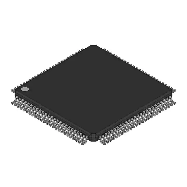
The 71V3557S75PFG 3.3V CMOS Synchronous SRAM is organized as 128K x 36. It is designed to eliminate dead bus cycles when turning the bus around between reads and writes, or writes and reads. Thus it has been given the name ZBTTM, or Zero Bus Turnaround. The 71V3557S75PFG contains address, data-in and control signal registers. The outputs are flow-through (no output data register).
Feature
- High performance system speed 100 MHz (7.5 ns Clock-to-Data Access)
- ZBTTM Feature - No dead cycles between write and read cycles
- Internally synchronized output buffer enable eliminates the need to control OE
- Single R/W (READ/WRITE) control pin
- 4-word burst capability (Interleaved or linear)
- Individual byte write (BW1 - BW4) control (May tie active)
- Three chip enables for simple depth expansion
- 3.3V power supply (±5%), 3.3V (±5%) I/O Supply (VDDQ)
- Optional Boundary Scan JTAG Interface (IEEE 1149.1 complaint)
- Available in 100-pin TQFP and 119-pin BGA packages


