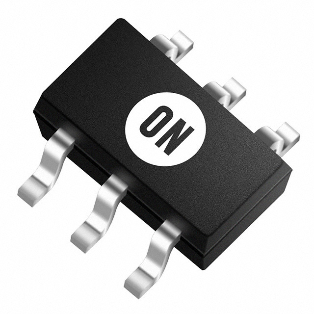
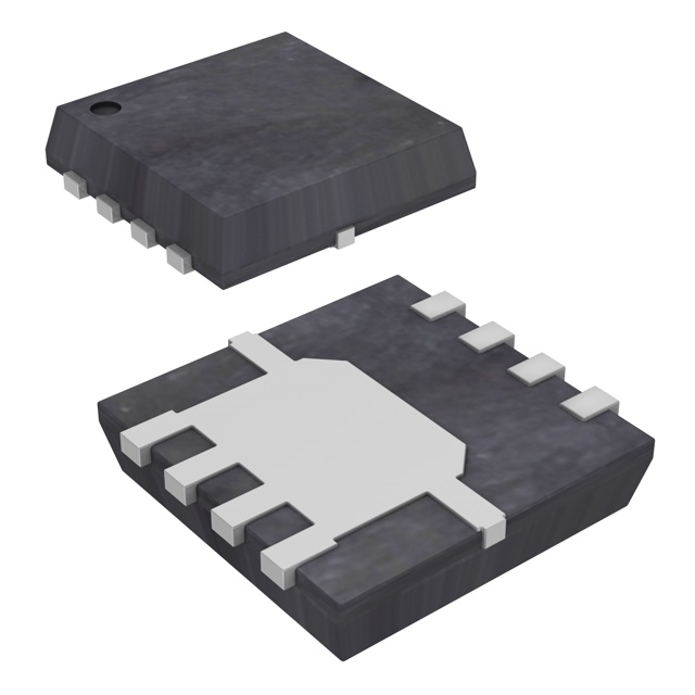
The NVT2008/NVT2010 are bidirectional voltage level translators operational from 1.0 V to 3.6 V (Vref(A)) and 1.8 V to 5.5 V (Vref(B)), which allow bidirectional voltage translations between 1.0 V and 5 V without the need for a direction pin in open-drain or push-pull applications. Bit widths of 8-bit to 10-bit are offered for level translation application with transmission speeds < 33 MHz for an open-drain system with a 50 pF capacitance and a pull-up of 197 Ω.
When the An or Bn port is LOW, the clamp is in the ON-state and a low resistance connection exists between the An and Bn ports. The low ON-state resistance (Ron) of the switch allows connections to be made with minimal propagation delay. Assuming the higher voltage is on the Bn port when the Bn port is HIGH, the voltage on the An port is limited to the voltage set by VREFA. When the An port is HIGH, the Bn port is pulled to the drain pull-up supply voltage (Vpu(D)) by the pull-up resistors. This functionality allows a seamless translation between higher and lower voltages selected by the user without the need for directional control.
When EN is HIGH, the translator switch is on, and the An I/O are connected to the Bn I/O, respectively, allowing bidirectional data flow between ports. When EN is LOW, the translator switch is off, and a high-impedance state exists between ports. The EN input circuit is designed to be supplied by Vref(B). To ensure the high-impedance state during power-up or power-down, EN must be LOW.
All channels have the same electrical characteristics and there is minimal deviation from one output to another in voltage or propagation delay. This is a benefit over discrete transistor voltage translation solutions, since the fabrication of the switch is symmetrical. The translator provides excellent ESD protection to lower voltage devices, and at the same time protects less ESD-resistant devices.
Feature
- Provides bidirectional voltage translation with no direction pin
- Less than 1.5 ns maximum propagation delay
- Allows voltage level translation between:
- 1.0 V Vref(A) and 1.8 V, 2.5 V, 3.3 V or 5 V Vref(B)
- 1.2 V Vref(A) and 1.8 V, 2.5 V, 3.3 V or 5 V Vref(B)
- 1.8 V Vref(A) and 3.3 V or 5 V Vref(B)
- 2.5 V Vref(A) and 5 V Vref(B)
- 3.3 V Vref(A) and 5 V Vref(B)
- Low 3.5 Ω ON-state connection between input and output ports provides less signal distortion
- 5 V tolerant I/O ports to support mixed-mode signal operation
- High-impedance An and Bn pins for EN = LOW
- Lock-up free operation
- Flow through pinout for ease of printed-circuit board trace routing
- ESD protection exceeds 4 kV HBM per JESD22-A114 and 1000 V CDM perJESD22-C101
- Packages offered: TSSOP20, DHVQFN20, TSSOP24, DHVQFN24, HVQFN24


