General Description
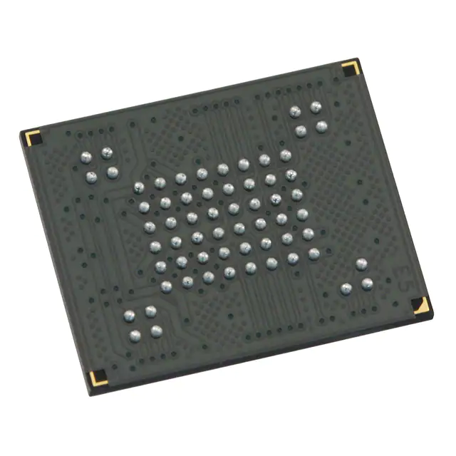
The serial peripheral interface (SPI) provides NAND Flash with a cost-effective non-volatile memory storage solution in systems where pin count must be kept to a minimum. It is also an alternative to SPI-NOR, offering superior write performance and cost per bit over SPI-NOR. SPI NAND Flash is an SLC NAND Flash memory device based on the standard parallel NAND Flash. The serial electrical interface follows the industry-standard serial peripheral interface. New command protocols and registers are defined for SPI operation. The command set resembles common SPI-NOR command sets, modified to handle NANDspecific functions and added new features. New features include user-selectable internal ECC. SPI NAND Flash devices have six signal lines plus VCC and ground (GND). The signal lines are SCK (serial clock), SI, SO (for command/response and data input/output), and control signals CS, HOLD#, WP#. This hardware interface creates a low-pincount device with a standard pinout that remains the same from one density to another, supporting future upgrades to higher densities without board redesign. Each block of the serial NAND Flash device is subdivided into 64 programmable pages. Each page consists of 2112 bytes. The pages are further divided into a 2048-byte data storage region with a separate 64-byte spare area. The 64-byte area is typically used for memory and error management functions. See Table 10 on page 32 for available user area when ECC is enabled. With internal ECC enabled, ECC code is generated internally when a page is written to the memory core. The ECC code is stored in the spare area of each page. When a page is read to the cache register, the ECC code is calculated again and compared with the stored value. Errors are corrected if necessary. The device either outputs corrected data or returns an ECC error status.
Features
(Picture:Pinout / Diagram)


