Features
· Open NAND Flash Interface(ONFI) 1.0-compliant1
· Single-level cell(SLC) technology
· Organization
-Page size x8:2112 bytes(2048+64 bytes)-Page sizex16:1056 words(1024+32 words)
-Block size:64 pages(128K+4K bytes)
-Plane size:2 planes x 2048 blocks per plane-Device size:4Gb:4096 blocks;8Gb:8192 blocks
16Gb:16,384 blocks
· Asynchronous I/O performance
-tRC/tWC:20ns (3.3V),25ns(1.8V)
· Array performance
-Read page:25us3
-Program page:200us(TYP:1.8V3.3V)3
-Erase block:700us(TYP)
· Command set: ONFI NAND Flash Protocol
· Advanced command set
-Program page cache mode4
-Read page cache mode 4
-One-time programmable(OTP) mode
-Two-plane commands 4
-Interleaved die(LUN) operations
-Read unique ID
-Block lock(1.8Vonly)
-Internal data move
· Operation status byte provides software method for detecting
-Operation completion
-Pass/fail condition
-Write-protect status
· Ready/Busy#(R/B#) signal provides a hardware method of detecting operation completion
· WP# signal: Write protect entire device
· First block(block address 00h) is valid when shipped from factory with ECC. For minimum required ECC, see Error Management.
· Block 0 requires 1-bit ECC if PROGRAM/ERASE cycles are less than 1000
· RESET(FFh) required as first command after power-on
· Alternate method of device initialization(Nand_In it) after power up(contact factory)
· Internal data move operations supported within the plane from which data is read
· Quality and reliability-Data retention:10 years
-Endurance:100,000 PROGRAM/ERASE cycles
· Operating voltage range
-Vcc:2.7-3.6V
-Voc:1.7-1.95V
· Operating temperature:
-Commercial:0℃ to+70℃
-Industrial(IT):-400C to+85C
· Package
-48-pin TSOP type 1, CPL2
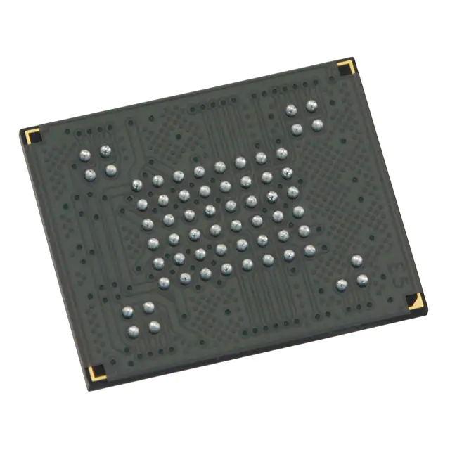
-63-ball VFBGA
(Picture:Pinout / Diagram)


