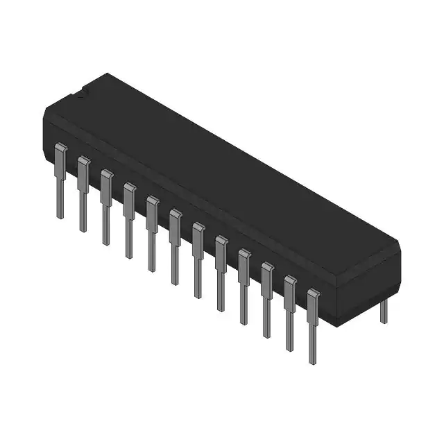
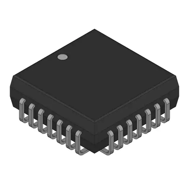
The GAL22LV10D, at 4 ns maximum propagation delay time, provides the highest speed performance available in the PLD market. The GAL22LV10C can interface with both 3.3V and 5V signal levels. The GAL22LV10Z-15QJ is manufactured using Lattice Semiconductor's advanced 3.3V E2 CMOS process, which combines CMOS with Electrically Erasable (E2 ) floating gate technology. High speed erase times (<100ms) allow the devices to be reprogrammed quickly and efficiently.
The generic architecture provides maximum design flexibility by allowing the Output Logic Macrocell (OLMC) to be configured by the user.
Unique test circuitry and reprogrammable cells allow complete AC, DC, and functional testing during manufacture. As a result, Lattice Semiconductor delivers 100% field programmability and functionality of all GAL products. In addition, 100 erase/write cycles and data retention in excess of 20 years are specified.
Feature
• HIGH PERFORMANCE E2CMOS® TECHNOLOGY
— 4 ns Maximum Propagation Delay
— Fmax = 250 MHz
— 3 ns Maximum from Clock Input to Data Output
— UltraMOS® Advanced CMOS Technology
• 3.3V LOW VOLTAGE 22V10 ARCHITECTURE
— JEDEC-Compatible 3.3V Interface Standard
— 5V Compatible Inputs
— I/O Interfaces with Standard 5V TTL Devices (GAL22LV10C)
• ACTIVE PULL-UPS ON ALL PINS (GAL22LV10D)
• E2 CELL TECHNOLOGY
— Reconfigurable Logic
— Reprogrammable Cells
— 100% Tested/100% Yields
— High Speed Electrical Erasure (<100ms)
— 20 Year Data Retention
• TEN OUTPUT LOGIC MACROCELLS
— Maximum Flexibility for Complex Logic Designs
— Programmable Output Polarity
• PRELOAD AND POWER-ON RESET OF ALL REGISTERS
— 100% Functional Testability
Applications
— Glue Logic for 3.3V Systems
— DMA Control
— State Machine Control
— High Speed Graphics Processing
— Standard Logic Speed Upgrade
(Picture: Pinout)


