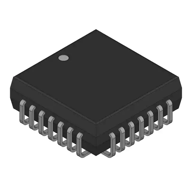
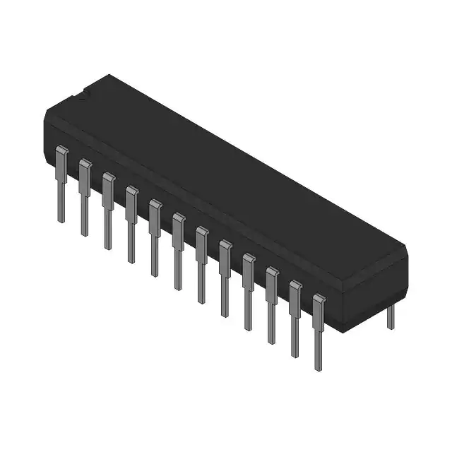
The GAL20V8-25LVC , at 5ns maximum propagation delay time, combines a high performance CMOS process with Electrically Eras-able(E2) floating gate technology to provide the highest speed performance available in the PLD market High speed erase times
(<100ms) allow the devices to be reprogrammed quickly and efficiently.
The generic architecture provides maximum design flexibility by allowing the Output Logic Macrocell (OLMC) to be configured by the user. An important subset of the many architecture configura-tions possible with the GAL20V8 are the PAL architectures listed in the table of the macrocell description section. GAL20V8-25LVC devices are capable of emulating any of these PAL architectures with full function/fuse map/parametric compatibility.
Unique test circuitry and reprogrammable cells allow complete AC, DC, and functional testing during manufacture. As a result, Lattice Semiconductor delivers 100% field programmability and functionality of all GAL products. In addition,100 erase/write cycles and data retention in excess of 20 years are specified.
Feature
• HIGH PERFORMANCE E2CMOS® TECHNOLOGY
— 5 ns Maximum Propagation Delay
— Fmax = 166 MHz
— 4 ns Maximum from Clock Input to Data Output
— UltraMOS® Advanced CMOS Technology
• 50% to 75% REDUCTION IN POWER FROM BIPOLAR
— 75mA Typ Icc on Low Power Device
— 45mA Typ Icc on Quarter Power Device
• ACTIVE PULL-UPS ON ALL PINS
• E2 CELL TECHNOLOGY
— Reconfigurable Logic
— Reprogrammable Cells
— 100% Tested/100% Yields
— High Speed Electrical Erasure (<100ms)
— 20 Year Data Retention
• EIGHT OUTPUT LOGIC MACROCELLS
— Maximum Flexibility for Complex Logic Designs
— Programmable Output Polarity
— Also Emulates 24-pin PAL® Devices with Full Function/ Fuse Map/Parametric Compatibility
• PRELOAD AND POWER-ON RESET OF ALL REGISTERS
— 100% Functional Testability
Applications
— DMA Control
— State Machine Control
— High Speed Graphics Processing
— Standard Logic Speed Upgrade
(Picture: Pinout)


